What are Micro Surgical Blade, Crescent Blade, and Keratome?
In modern ophthalmic microsurgery, precision is everything. Instruments such as micro surgical blades, crescent blades, and keratomes require extremely sharp edges, consistent geometry, and flawless surface quality. Even the smallest imperfection can affect surgical performance.
So how are these ultra-precision blades manufactured?
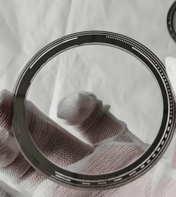
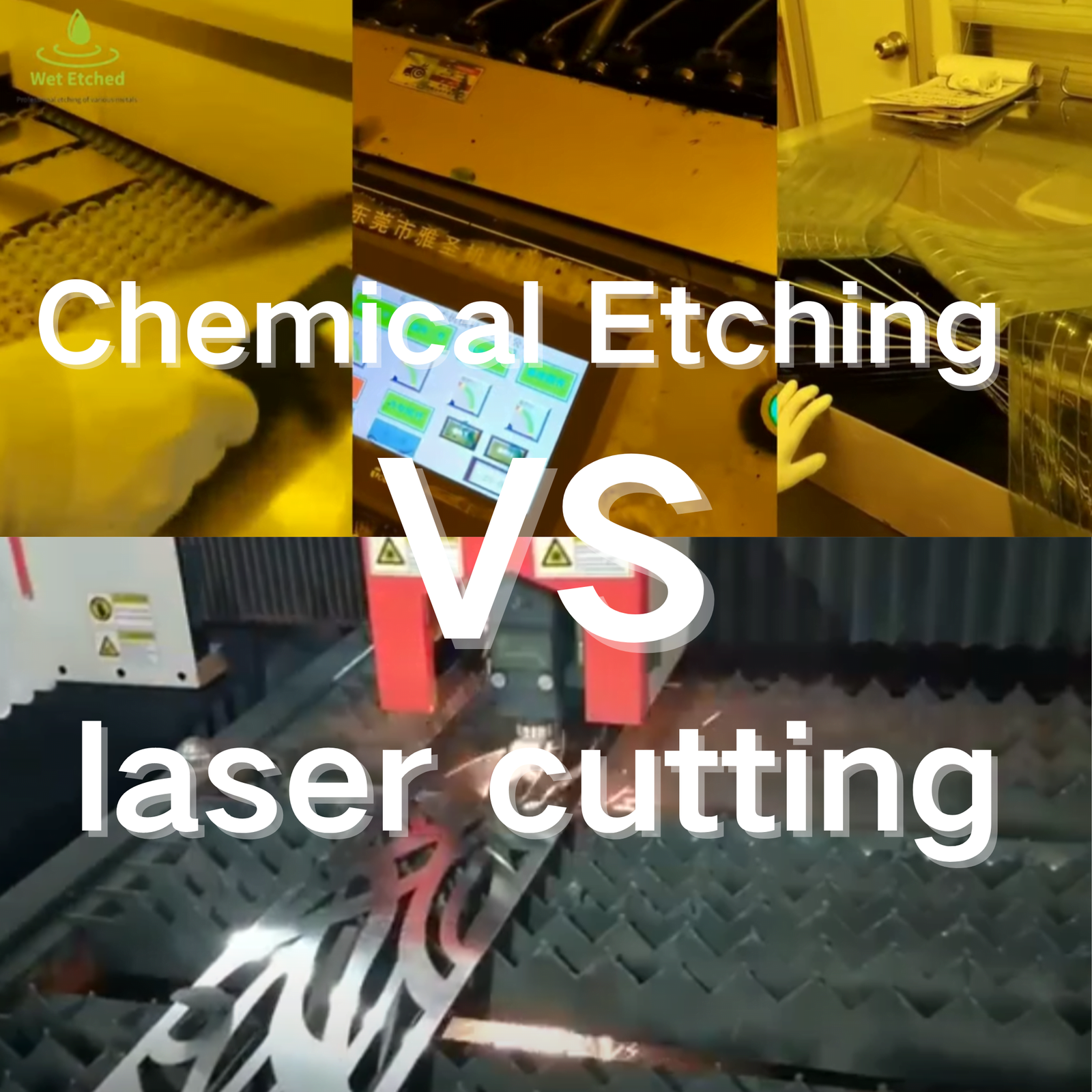
One of the most advanced and reliable methods today is chemical etching, also known as photo chemical machining (PCM). This process enables manufacturers to produce high-precision surgical components with unmatched consistency and flexibility.
What Are Micro Surgical Blades?
Micro surgical blades are specialized cutting tools designed for delicate procedures, especially in ophthalmology. Common types include:
- Micro surgical blades – general-purpose precision cutting tools
- Crescent blades – used for lamellar dissection with curved cutting edges
- Keratomes – designed for precise corneal incisions
These instruments must meet strict requirements in terms of sharpness, edge uniformity, and dimensional accuracy.
Why Chemical Etching Is Ideal for Blade Manufacturing
Unlike traditional machining methods such as CNC grinding or laser cutting, chemical etching removes material without mechanical force. This provides several critical advantages:
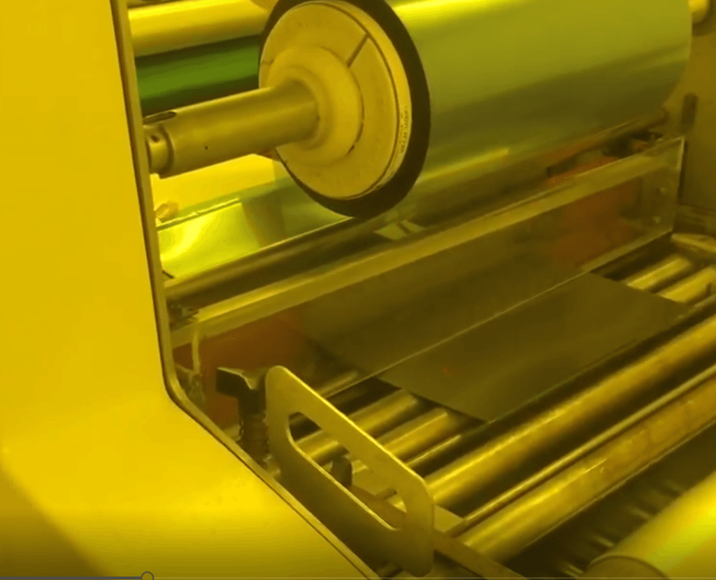
How is it processed using chemical etching?
Taking SUS316 stainless steel as an example, a few seconds of animation will give you an understanding of the chemical etching process.
1. No Mechanical Stress
There is no tool contact during the etching process, which eliminates deformation and preserves the integrity of thin metal parts.
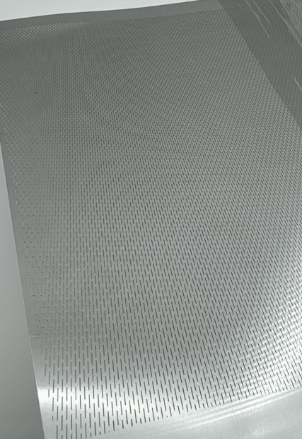
2. Burr-Free Edges
Chemical etching produces clean, smooth edges without secondary deburring operations — essential for medical-grade blades.
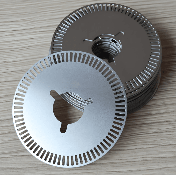
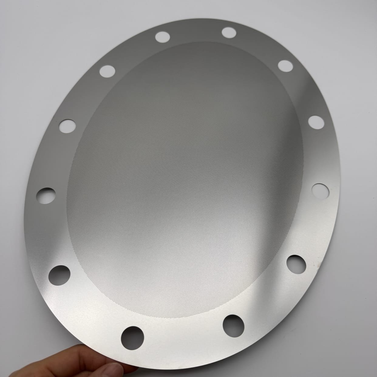
3. Complex Geometry Capability
Intricate blade shapes, including curved and micro-scale features, can be achieved with high precision.
4. High Repeatability
The process ensures consistent results across large production volumes, making it suitable for both prototyping and mass manufacturing.
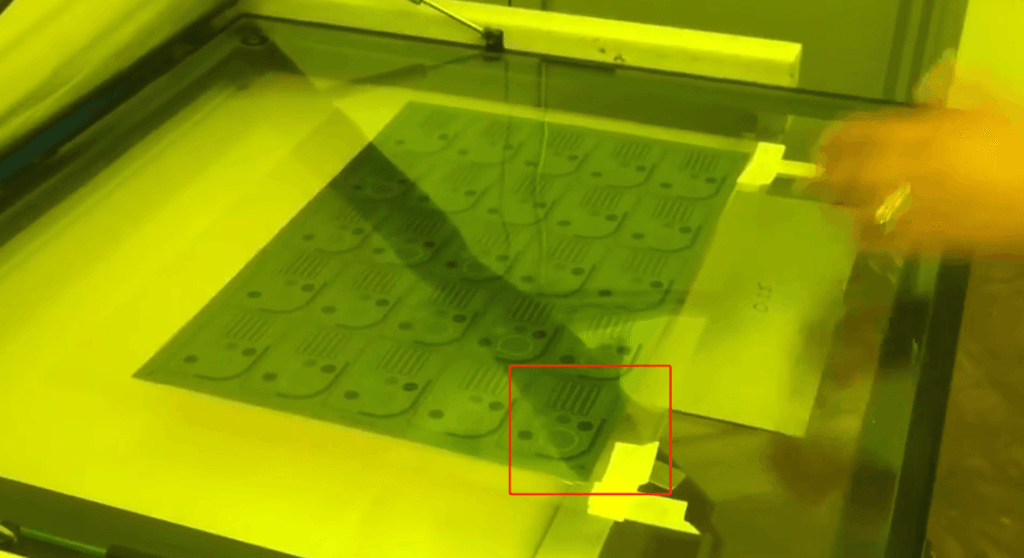
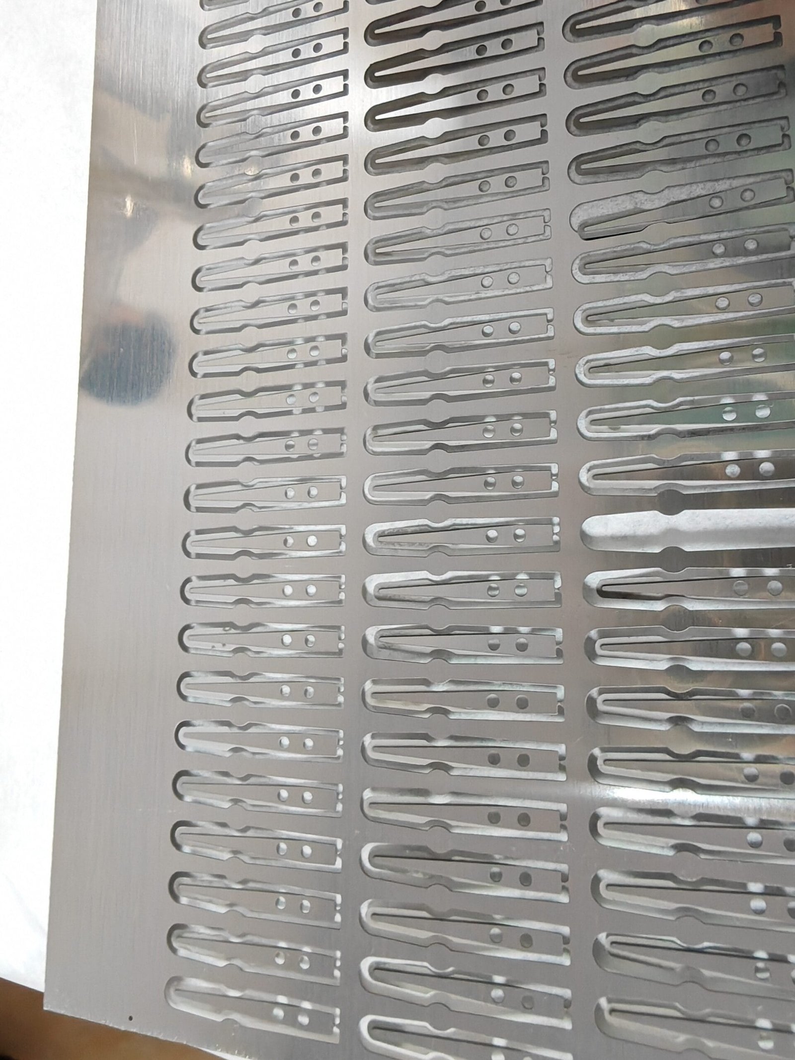
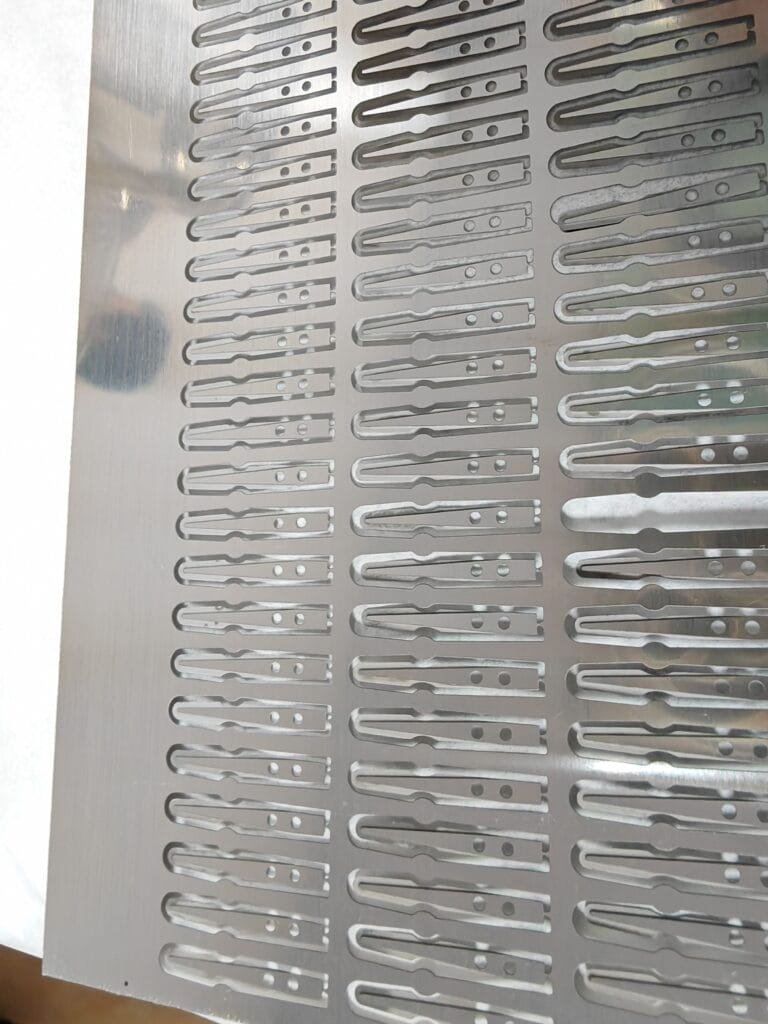
From Etching to Finished Blade Video

The manufacturing process typically includes the following steps:
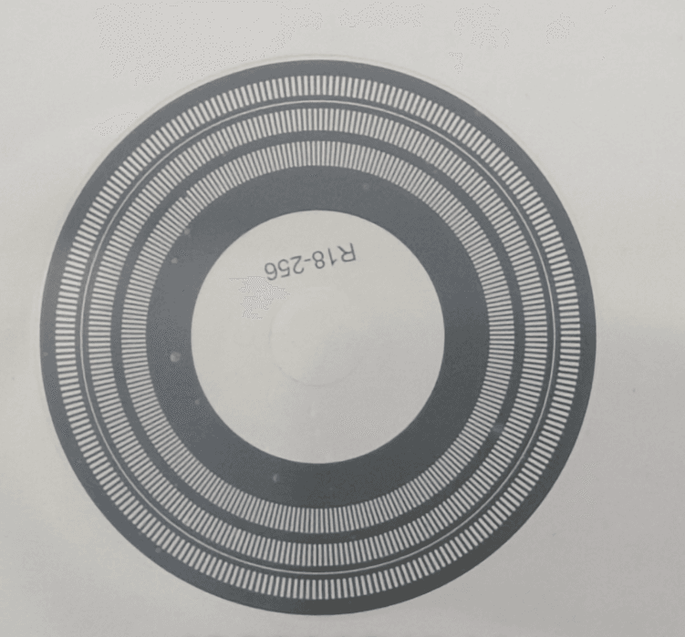
- Material Preparation
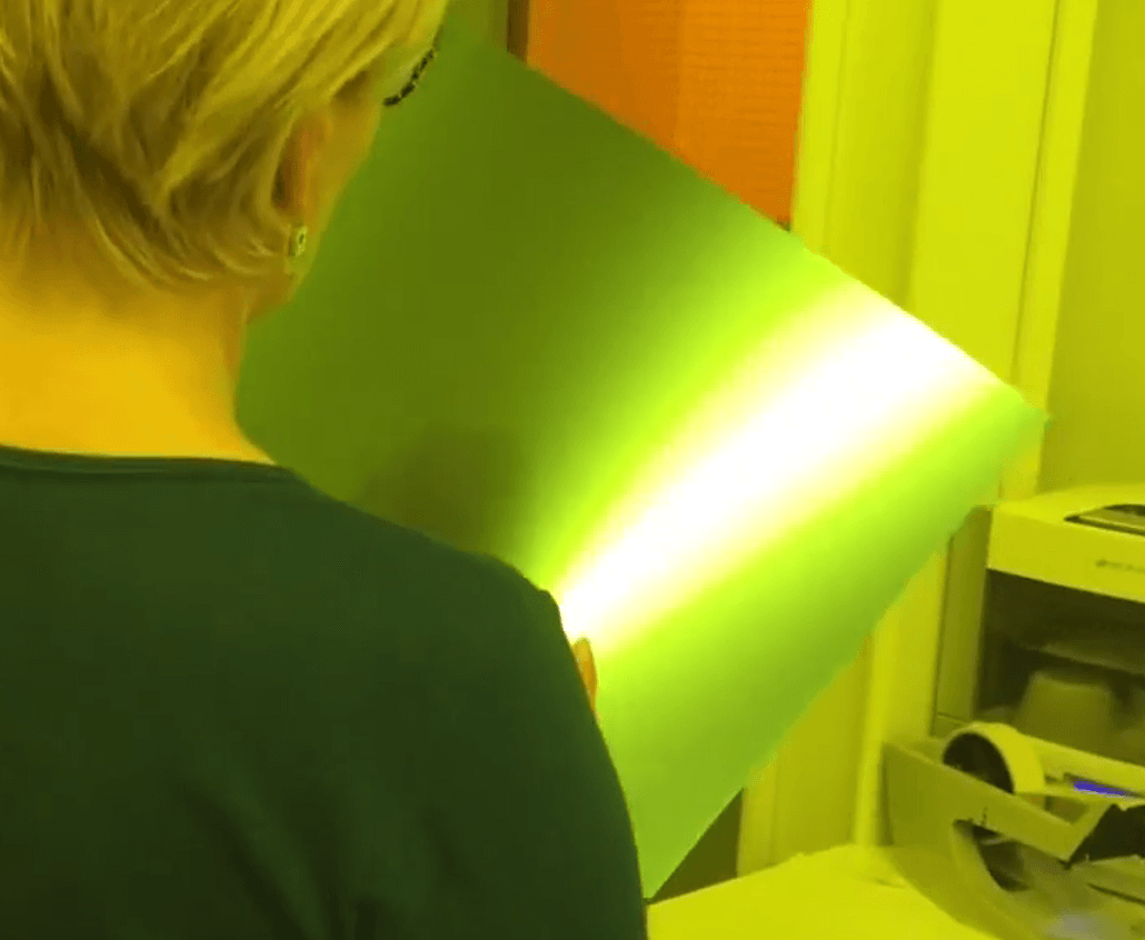
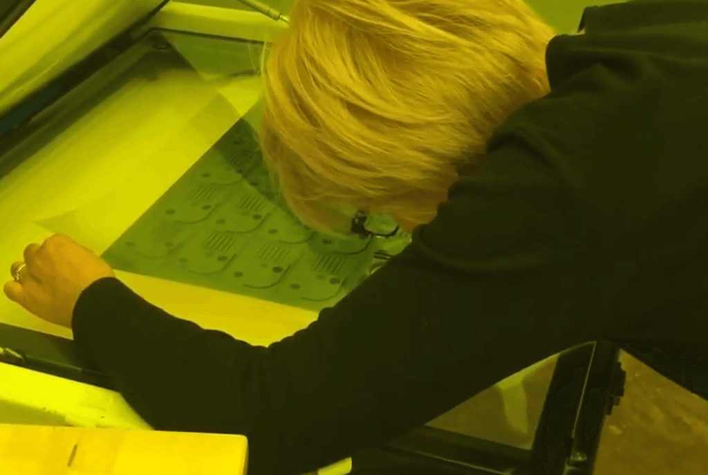
High-quality metal sheets (such as stainless steel) are selected based on application requirements. - Photoresist Coating & Exposure
A patterned mask defines the blade geometry with micron-level accuracy. - Chemical Etching
Controlled chemical reactions remove unwanted material to form the blade profile. - Stripping and Cleaning
After etching, the blades are released (stripped) from the sheet and thoroughly cleaned. - Final Inspection
Each blade is checked for dimensional accuracy and edge quality.
This process ensures that every blade meets strict precision standards without introducing defects.
Performance Validation: Initial Penetration Test
To evaluate blade performance, manufacturers often conduct an initial penetration test.
This test measures how easily a blade can enter a controlled material, simulating resistance similar to soft tissue. It provides a reliable indication of:
- Edge sharpness
- Penetration efficiency
- Cutting consistency
A blade with lower penetration resistance typically delivers better performance in real-world applications, reducing the force required during use.
Chemical Etching vs Traditional Manufacturing
| Feature | Chemical Etching | CNC Machining / Laser Cutting |
|---|---|---|
| Mechanical Stress | None | Present |
| Burr Formation | None | Requires secondary processing |
| Precision | High (micro-level) | Moderate to high |
| Tooling Cost | Low | High |
| Design Flexibility | Excellent | Limited for complex geometries |
This makes chemical etching especially suitable for medical blades and precision components.
Equipment and Manufacturing Solutions
For companies looking to enter or scale micro blade production, investing in the right equipment is critical.
We provide:
- Advanced chemical etching machines for precision metal processing
- Complete production lines including cleaning, exposure, etching, and stripping
- Custom manufacturing services for micro surgical blades and other precision parts
Whether you are a medical device manufacturer, a precision engineering company, or a startup developing new products, chemical etching offers a scalable and cost-effective solution.
Why Choose Chemical Etching for Micro Blades
- No tooling cost for rapid design iteration
- Ideal for both prototypes and high-volume production
- Superior edge quality and consistency
- Capability to handle ultra-thin materials
In an industry where precision directly impacts performance, chemical etching stands out as a reliable and future-ready manufacturing method.