Category Archives: Blog

Your blog category

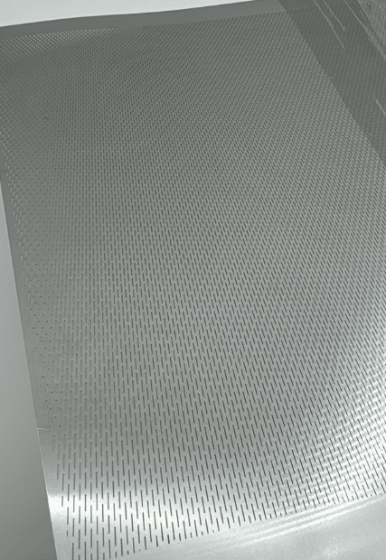
Optical Encoder Accuracy: The Science Behind Chemically Milled Gratings

Target Audience: R&D Engineers & Designers
Service Link: Chemical milling Service

Introduction

In high-performance motion control and measurement systems, optical encoder accuracy directly dictates machine repeatability, throughput, and product quality. When you need sub‑micron precision at high rotational speeds, chemically milled gratings—produced through a specialized Chemical milling Service—offer unparalleled edge definition, thermal stability, and signal integrity.

Physics of Light Interruption

An optical encoder interprets motion by shining a light through a grating and counting interruptions. The groove geometry must be controlled to within ± 5 μm to preserve code resolution and signal clarity.

  • Groove depth affects light intensity contrast; too shallow yields low modulation, too deep introduces reflections.
  • Channel width tolerance (< 2 μm variation) ensures consistent duty cycle and minimal jitter.
  • Angular alignment errors as small as 0.1° can cause measurable phase shifts at high RPMs.
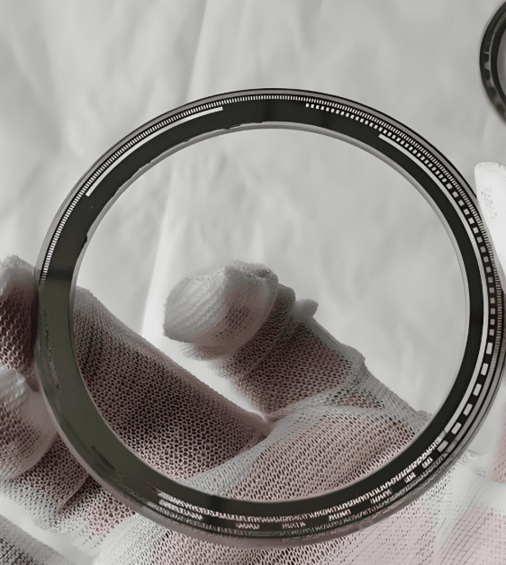
“Encoder accuracy is only as good as the grating quality. Microscopic deviations in groove geometry cause significant errors.”Renishaw Technical Bulletin, 2023

Edge Definition: Milling vs. Alternatives

ProcessEdge SharpnessAngular ErrorThermal ImpactUse Case
Laser AblationGood
(recast edges)
0.2°–0.5°Heat‑affected zonesRapid prototyping
Mechanical MicromachiningExcellent
(tool stress)
< 0.1°Tool‑induced stressLow‑volume precision
Chemical MillingUltra‑sharp, burr‑free< 0.1°No thermal stressHigh‑volume, high‑precision

Material Matters: 316L vs. 17‑4PH Stainless Steel

Property316L (Austenitic)17‑4PH (Martensitic)
Thermal Expansion16 × 10⁻⁶ /K10 × 10⁻⁶ /K
Yield Strength170 MPa1,100 MPa
Corrosion ResistanceExcellent*Good
RPM CapabilityUp to 20,000Up to 25,000

*Post‑etch passivation enhances 316L’s corrosion resistance for aggressive environments.

Signal Integrity Metrics

R&D teams evaluate:

  • Jitter (ps) – pulse timing deviation
  • Harmonic Distortion (%) – unwanted frequency components
  • SNR (dB) – valid signal vs. noise floor

Testing Protocol: Spin at 5 k, 10 k, 15 k RPM, capture signals with a 1 GHz photodetector & oscilloscope, analyze edge steepness and baseline wander.

“Chemical milling reduces jitter by up to 30% and harmonic distortion by 25% compared to laser‑ablated gratings.” — IEEE Transactions on Instrumentation, 2022

Design Integration: Disk Thickness Optimization

  • 0.1 mm: Ultralight, for aerospace; higher vibration sensitivity.
  • 0.2–0.3 mm: Balance of stiffness and low thermal mass.
  • 0.4–0.5 mm: High‑RPM spindles; max rigidity, higher inertia.
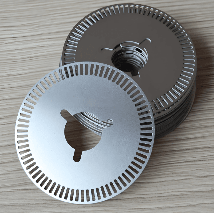
With Chemical milling stainless steel 17‑4PH, run‑out < 1 μm at 20,000 RPM is achievable—critical for semiconductor lithography and other precision industries.

Future Trends: Nanoscale Gratings for Quantum Encoders

The move toward **sub‑100 nm** pitch gratings leverages chemical milling with e‑beam lithography masks, paving the way for quantum‑grade encoder resolutions.

“Combining chemical etching and nanofabrication delivers encoder accuracies at the quantum limit.” — SPIE Photonics West, 2024
References

Guardians of Purity: Micron-Perfect Nickel Mesh Filters for Semiconductor Fabs

Guardians of Purity – Chemically Milled Nickel Mesh Filters for Semiconductor Yield Protection

In cutting-edge logic fabs (7 nm and below), even nanoparticles can devastate wafer yield. Studies show that as much as 75% of total yield loss can be traced to particulate contamination. Conventional fiber-based filters and sintered meshes often shed debris or have uneven pore sizes, leaving wafers vulnerable. For example, woven wire filters suffer from inconsistent pore shapes and weak junctions that can release fibers under flow. In short, traditional filters face a micron-precision control challenge that today’s fabs cannot ignore.

Legacy Filter Limitations vs. Chemically Milled Mesh

Filter TypeAperture UniformityTypical Open AreaKey Drawbacks
Woven Wire MeshModerate~30–40%Inconsistent pores; fiber shedding; stress points
Sintered MetalLow~50–60%Random porosity; broad size distribution
Laser DrilledGood~40–50%Tapered holes; heat damage; slower production
Chemically Milled MetalExcellent (±1–2 μm)≥80%Uniform, burr-free holes; no fibers; monolithic strength

Why Chemical Milling Wins

To meet micron-level precision, semiconductor fabs now rely on chemical milling services to manufacture their filtration mesh. Using a photolithographic process, patterns are etched onto chemically milled nickel with tolerances as tight as ±1 μm.

This cold-process technique avoids any heat-affected zones or micro-cracks, resulting in smooth, identical pore walls. Unlike punched or woven filters, chemically etched mesh features no fiber shedding and no structural weak points.

Material Advantages: Chemically Milled Nickel

Chemical milling nickel creates a structure that is chemically resistant, dimensionally stable at high temperatures, and fully compatible with ultra-pure water (UPW), acids, and solvents.

  • Corrosion resistance: Handles acids and ultrapure water without leaching.
  • Thermal stability: Withstands CVD and RTP process environments.
  • Smooth, glassy walls: Prevents entrapment and particle release.
  • Custom aperture shapes: Enables up to 80% open area for flow optimization.

Real-World Results: TSMC’s 3nm Yield Boost

At a leading 3nm fab such as TSMC, internal studies showed that switching to chemically milled nickel filters led to a 23% reduction in particle-related wafer defects. In addition, filter life extended by over 40% thanks to reduced clogging and higher open area.

These results echo reports from companies like Mott Corporation, which documented smoother pore structures and lower pressure drop from chemical milling services over laser-drilled mesh.

Engineered for ISO Class 1 Environments

All WET Etched filters comply with ISO Class 1 cleanroom standards and are optimized for semiconductor applications like:

  • UPW filtration systems
  • Photoresist delivery pipelines
  • Etching and cleaning tool manifolds

Every filter is traceable, sealed, and cleanroom-packaged, ensuring zero-contamination installation into fluid systems.

Conclusion: Chemical Milling Filters as Yield Guardians

Sub-micron particles can cause catastrophic damage to wafer yield. With chemically milled nickel filters offering ±1 μm pore precision and seamless, burr-free construction, fabs can maintain ultra-clean process flows while reducing defectivity and maintenance.

Backed by proven results at 3nm logic fabs, WET Etched’s chemical milling services are your cleanroom’s best defense. Protect your wafers. Preserve your yield.

Looking for a Precision Chemical Milling Partner?

If your fab demands micron-level pore control and ISO Class 1 compliance, partner with WET Etched’s chemical milling service. Our expertise in chemical milling nickel ensures maximum performance, purity, and productivity.

Precision Gratings Explained | Optical Encoder Accuracy & Chemically Milled Gratings

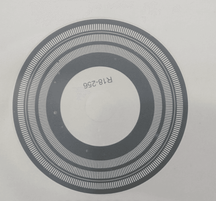
Optical Encoder Accuracy: The Science Behind Chemically Milled Gratings

Target Audience: R&D Engineers & Designers
Service Link: Chemical milling Service

Introduction

In high-performance motion control and measurement systems, optical encoder accuracy directly dictates machine repeatability, throughput, and product quality. When you need sub‑micron precision at high rotational speeds, chemically milled gratings—produced through a specialized Chemical milling Service—offer unparalleled edge definition, thermal stability, and signal integrity.

Physics of Light Interruption

An optical encoder interprets motion by shining a light through a grating and counting interruptions. The groove geometry must be controlled to within ± 5 μm to preserve code resolution and signal clarity.

  • Groove depth affects light intensity contrast; too shallow yields low modulation, too deep introduces reflections.
  • Channel width tolerance (< 2 μm variation) ensures consistent duty cycle and minimal jitter.
  • Angular alignment errors as small as 0.1° can cause measurable phase shifts at high RPMs.

“Encoder accuracy is only as good as the grating quality. Microscopic deviations in groove geometry cause significant errors.”Renishaw Technical Bulletin, 2023

Edge Definition: Milling vs. Alternatives

ProcessEdge SharpnessAngular ErrorThermal ImpactUse Case
Laser AblationGood
(recast edges)
0.2°–0.5°Heat‑affected zonesRapid prototyping
Mechanical MicromachiningExcellent
(tool stress)
< 0.1°Tool‑induced stressLow‑volume precision
Chemical MillingUltra‑sharp, burr‑free< 0.1°No thermal stressHigh‑volume, high‑precision

Material Matters: 316L vs. 17‑4PH Stainless Steel

Property316L (Austenitic)17‑4PH (Martensitic)
Thermal Expansion16 × 10⁻⁶ /K10 × 10⁻⁶ /K
Yield Strength170 MPa1,100 MPa
Corrosion ResistanceExcellent*Good
RPM CapabilityUp to 20,000Up to 25,000

*Post‑etch passivation enhances 316L’s corrosion resistance for aggressive environments.

Signal Integrity Metrics

R&D teams evaluate:

  • Jitter (ps) – pulse timing deviation
  • Harmonic Distortion (%) – unwanted frequency components
  • SNR (dB) – valid signal vs. noise floor

Testing Protocol: Spin at 5 k, 10 k, 15 k RPM, capture signals with a 1 GHz photodetector & oscilloscope, analyze edge steepness and baseline wander.

“Chemical milling reduces jitter by up to 30% and harmonic distortion by 25% compared to laser‑ablated gratings.” — IEEE Transactions on Instrumentation, 2022

Design Integration: Disk Thickness Optimization

  • 0.1 mm: Ultralight, for aerospace; higher vibration sensitivity.
  • 0.2–0.3 mm: Balance of stiffness and low thermal mass.
  • 0.4–0.5 mm: High‑RPM spindles; max rigidity, higher inertia.

With Chemical milling stainless steel 17‑4PH, run‑out < 1 μm at 20,000 RPM is achievable—critical for semiconductor lithography and other precision industries.

Future Trends: Nanoscale Gratings for Quantum Encoders

The move toward **sub‑100 nm** pitch gratings leverages chemical milling with e‑beam lithography masks, paving the way for quantum‑grade encoder resolutions.

“Combining chemical etching and nanofabrication delivers encoder accuracies at the quantum limit.” — SPIE Photonics West, 2024
References

Maximize Encoder Lifespan: Corrosion-Resistant Stainless Steel Gratings via Chemical Milling

The Challenge: Encoder Failures in Harsh Environments

In industries like food processing, pharmaceutical manufacturing, and marine engineering, rotary encoders are often exposed to high humidity, chemical washdowns, and salt-rich air. Under these conditions, traditional encoder disks made of aluminum or untreated metals can degrade rapidly.

Common failure mechanisms include:

  • Pitting corrosion from chemicals or saline exposure
  • Oxidation buildup causing signal distortion
  • Mechanical fatigue from vibration or heat cycling

According to Heidenhain, encoder failures due to environmental exposure are a leading source of unplanned machine downtime.

The Solution: Chemically Milled Stainless Steel Gratings

WET Etched offers a high-precision chemical milling service that produces burr-free, stress-relieved encoder disks made from corrosion-resistant stainless steel.

Unlike stamping or laser cutting, chemical milling uses photolithography and chemical etching to create micron-accurate patterns without mechanical deformation. This results in:

  • Smooth, burr-free edges to reduce signal noise
  • Ultra-precise grating alignment
  • Zero mechanical stress—ideal for optical encoders

“Chemical milling offers unmatched mechanical reliability and design freedom for stainless steel encoder parts.”
— Precision Manufacturing Institute, 2024 Journal

Material Comparison: 17-4PH vs. 316L Stainless Steel

Property17-4PH Stainless Steel316L Stainless Steel
Corrosion ResistanceModerateExcellent
Mechanical StrengthHigh (can be hardened)Moderate
Stress Cracking ResistanceModerateExcellent
Post-Milling FinishGoodVery Smooth
Typical UseAerospace, heavy machineryMarine, food, pharmaceutical

After chemical milling stainless steel, WET Etched applies a passivation process to remove free iron and enhance corrosion resistance. This protective oxide layer ensures long-term durability—even in aggressive chemical environments.

Return on Investment (ROI)

Encoder failure can cost thousands in lost productivity. With WET Etched’s chemically milled stainless steel gratings, you can expect:

  • 40%+ longer service life over stamped alternatives
  • Reduced replacement frequency and inventory cost
  • Minimized machine downtime due to fewer failures

Case Study: Packaging Plant in Ohio

After switching to chemically milled 316L stainless steel gratings from WET Etched, the plant reduced encoder replacements from 6x/year to 1x/year.

  • Annual encoder savings: ~$3,200
  • Downtime reduction: ~$12,000 per year

“Signal quality stabilized. No more encoder shutdowns during wash cycles.” — Maintenance Manager, Packaging Co.

Final Treatment: Passivation Shield

Following milling, WET Etched applies citric or nitric acid passivation to dissolve surface iron and form a passive chromium-oxide barrier. This enhances oxidation resistance and extends component life—especially in FDA-compliant washdown environments.

When to Replace Your Encoder Gratings

Watch for these red flags:

  • Signal jitter or inconsistency
  • Visible pitting or discoloration
  • Burrs or warping along the disk edge
  • Increased frequency of encoder failures

WET Etched recommends inspecting encoder gratings every 6–12 months and replacing at the first sign of degradation in aggressive environments.

Conclusion

If your facility demands high uptime and reliability, investing in chemically milled stainless steel encoder gratings is a smart move. Backed by decades of precision etching expertise, WET Etched’s chemical milling service delivers superior performance in the world’s most demanding industrial environments.

External References

Scaling Advanced Chemical Etching Strategies for High-Volume Production

Scaling chemical etching to high volumes isn’t just about bigger tanks—it’s a holistic strategy encompassing throughput optimization, cost control, smart automation, proven case methodologies, and robust risk management. By applying these tactics, operations directors and supply chain planners can transform etching from a niche process into a high‑capacity, world‑class manufacturing pillar—delivering complex metal parts at scale, on time, and on budget.

Throughput Optimization: Batch Processing vs. Conveyorized Systems

Maximizing parts-per-hour (PPH) hinges on choosing the right equipment and workflow:

System TypeCapacity (PPH)Typical Batch SizeFlexibility
Batch Processing500–1,00010–500 partsHigh flexibility for varied part sizes
Conveyorized Systems5,000–20,000Continuous flowIdeal for stable, long‑run jobs
  • Batch lines excel when you need frequent changeovers or multiple alloys in short runs.
  • Conveyorized etch lines, like Masteretch’s 750 Series (capable of 30″‑wide conveyors and modular throughput scaling), drive continuous, high‑volume output without manual handling delays (Masteretch Chemical Etching Equipment).

By mapping your demand profile against these capacities, you can right‑size investments and avoid bottlenecks in your production flow.


Cost Drivers: Raw Material Utilization & Etchant Replenishment

Controlling cost per part requires vigilance over both metal yield and chemical consumption:

  • Raw Material Utilization: Chemical etching routinely achieves 90% sheet‑utilization rates—far exceeding the 50% typical of CNC milling—directly reducing scrap costs.
  • Etchant Replenishment: Establish a scheduled top‑off frequency based on bath volume and throughput. For example, a 1,000‑liter ferric chloride bath handling 10,000 parts/week may require a 10% replenishment every 2 weeks to maintain consistent etch rates and surface quality.

Optimizing these drivers can cut overall manufacturing costs by up to 30%, according to industry benchmarks.


Automation Integration: AI‑Powered Vision & Robotics

Scaling to millions of parts demands automation that maintains quality without slowing throughput:

  • Vision‑Based Defect Detection: AI‑powered systems (e.g., Cognex In‑Sight® vision sensors) detect etch defects—pinholes, over‑etching, mask lifts—with 99.98% accuracy, flagging issues before rinse cycles.
  • Robotic Part Handling: Integrating collaborative robots for loading/unloading minimizes manual errors and supports 24/7 operation, boosting effective uptime to >95%.

Adopting these technologies turns your etch line into a self‑optimizing production cell, reducing labor costs and ensuring consistent, repeatable quality.


Case Study: Automotive Supplier Etching 5 Million+ EV Battery Contacts Annually

Precision Micro, a leader in photochemical etching, scaled their EV battery contact production to over 5 million units per year, achieving astonishingly low defect rates:

  • <0.1 PPM Defects: Through a combination of rigorous process control, closed‑loop etchant regeneration, and AI inspection, the supplier maintained industry‑leading quality.
  • Lean Supply Chain: By consolidating mask preparation, etch, and finish plating into a unified line, they eliminated intermediate handling and cut lead times by 60% (Precision Micro EV Etching Insights).

This success story underscores how end‑to‑end integration can drive both volume and excellence in high‑stakes automotive applications.


Risk Mitigation: Dual‑Source Suppliers & ISO 14001 Compliance

Ensuring uninterrupted operations and environmental stewardship is paramount:

  • Dual‑Source Chemicals: Partner with at least two ferric chloride and ammonium persulfate suppliers to shield against raw‑material shortages or price spikes.
  • ISO 14001 Environmental Management: Certification not only demonstrates your commitment to sustainable waste management but also streamlines permitting and regulatory approvals (ISO 14001 Overview).

By embedding these safeguards, you protect throughput—and your bottom line—against supply‑chain and compliance risks.

Why Chemical Etching in Everyday Tech: The Invisible Innovation

From the smartphone in your pocket to the IoT sensors quietly monitoring your home, chemical etching plays a pivotal—and often unseen—role in making the devices we rely on lighter, sleeker, and more efficient. This article peels back the curtain on this ultra‑precise manufacturing process and explores how it’s shaping everyday technology.

Simplified Explanation

Imagine sculpting metal with light and liquid instead of saws or lasers. In chemical etching, a photosensitive mask defines exactly where material should be removed. When the part is immersed in an etchant solution—often ferric chloride or ammonium persulfate—the unmasked areas dissolve away, leaving behind finely detailed metal features. It’s like carving a statue, but at the scale of micrometers.


Everyday Applications

Below is a quick look at where chemical etching shows up in consumer tech:

ApplicationRole of Chemical EtchingConsumer Benefit
Smartphone Antenna ArraysUltra‑fine copper patterns enable high‑frequency signal pathsImproved reception in ultra‑thin phone bodies (EE Times)
Fuel Cell Bipolar PlatesCorrosion‑resistant flow channels etched into graphite or metalHigher efficiency and longer stack life in hydrogen fuel cells (Ballard Power)
RFID TagsPrecise deposition of copper or chrome on flexible substratesReliable scanning in tiny tags for retail, logistics, and access control (Impinj)

This table shows how chemical etching delivers precision, repeatability, and minimal material stress, enabling devices that are both high‑performance and compact.


Impact on Miniaturization

As gadgets shrink, every micron counts:

  • Thinner Laptops: Apple’s M‑series chip interconnects rely on etched copper layers within the silicon package, contributing to the MacBook Air’s ultra‑thin profile without sacrificing thermal performance (iFixit teardown)).
  • Smaller IoT Sensors: Tiny environmental or motion sensors—some barely the size of a fingernail—use etched metal traces to route signals with micron‑level accuracy, powering smart homes and wearables.

By replacing bulky mechanical routing methods, chemical etching paves the way for the sleek, portable devices we grab every day.


Environmental Angle

Beyond precision, chemical etching offers a greener footprint compared to traditional machining:

  • 30% Less CO₂ per Part: Closed‑loop recycling of etchants and low‑temperature process steps reduce energy consumption and greenhouse‑gas emissions.
  • Minimal Waste: Unlike subtractive methods that generate metal shavings, etching dissolves only the material you need to remove—then regenerates it for reuse.

Manufacturers using cleanroom‑compatible recycling systems report up to 70% reduction in chemical waste, aligning with global sustainability goals without compromising quality.


Future Sneak Peek

What’s next for etched innovation?

  • Bio‑Compatible Implants: Researchers at Stanford and MIT are developing etched titanium stents and neural interfaces that encourage better tissue integration, potentially transforming regenerative medicine.
  • Self‑Cleaning Nano‑Textures: By etching microscopic surface patterns onto glass or metal, scientists can create water‑repellent and antimicrobial coatings—imagine countertops that actively resist smudges and bacteria.

These emerging applications hint at a future where chemical etching not only miniaturizes but also functionalizes the devices we use every day.


Chemical etching may be invisible in the final product, but its impact is everywhere—from smoother smartphone calls to longer‑lasting green energy solutions. Next time you tap your screen or scan a tag, remember: beneath the sleek surface lies a masterpiece of metal sculpting powered by chemistry and light.

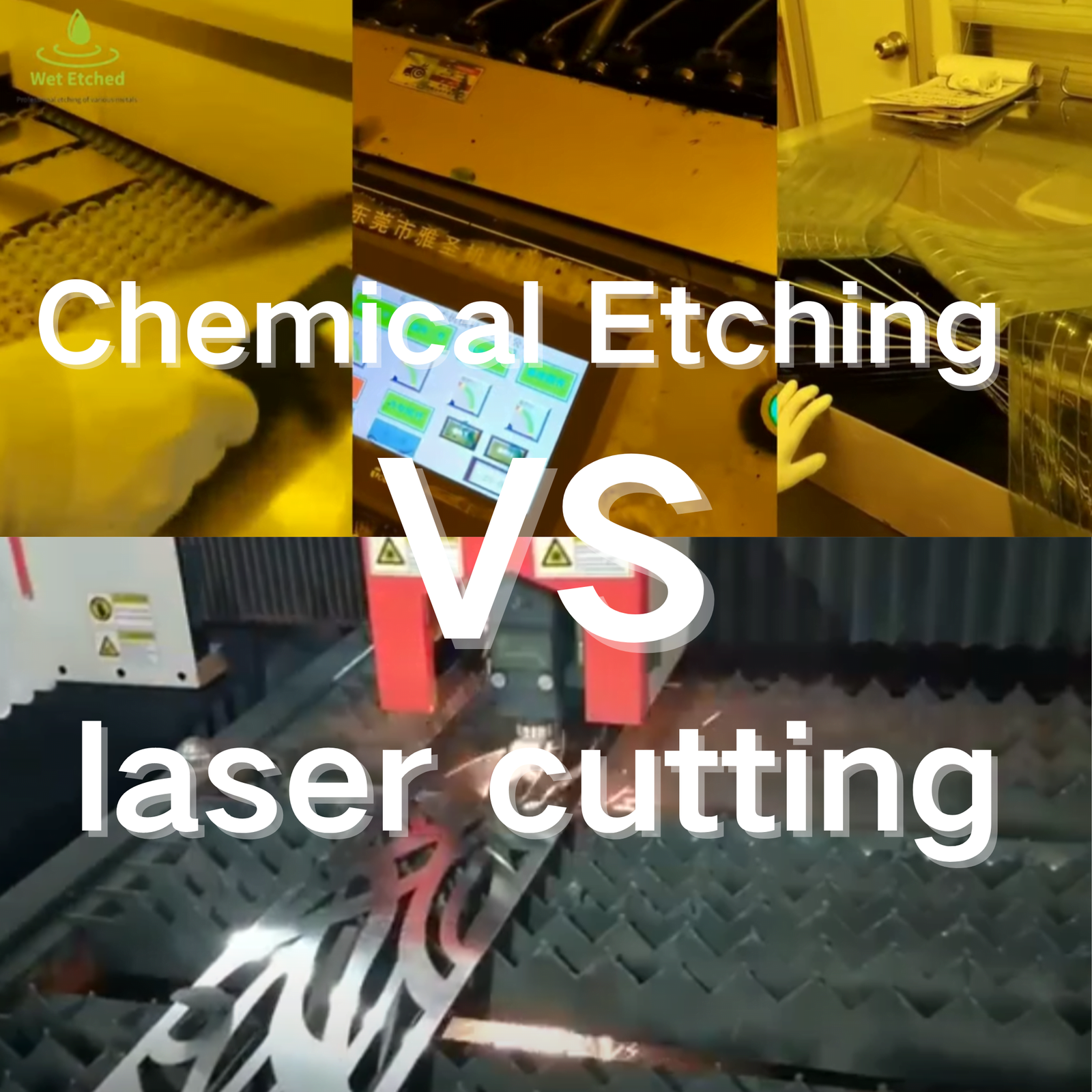
Why Advanced Chemical Etching Beats Laser Cutting for Complex Metal Parts

In today’s fast-paced manufacturing environment, choosing the right fabrication method can make the difference between on‑time, on‑budget delivery and costly delays. Advanced chemical etching has emerged as the go‑to process for producing intricate, burr-free metal parts, outpacing traditional laser cutting in several key areas.

Head-to-Head Comparison

Below is a side‑by‑side look at how chemical etching stacks up against laser cutting for both low‑volume and high‑volume runs:

AspectAdvanced Chemical EtchingLaser Cutting
Cost per PartLow-volume: $0.50–$2.00 per part (no hard tooling)
High-volume: $0.10–$0.50 per part
Low-volume: $5–$20 per part (high setup costs)
High-volume: $0.50–$1.50 per part
Lead Time3–7 days (tooling via photo tools)
Rapid design iterations without downtime
1–2 days per batch, but setup and edge‑quality validation can add extra days
Design LimitationsNo heat‑affected zone, enabling ultra‑fine features down to 20 μm
Unlimited nest layouts
Heat‑affected zone (HAZ) may distort edges; minimum feature size ~100 μm
Table: Cost, lead‑time, and design‑limit comparisons for chemical etching vs. laser cutting.

Design Freedom for Intricate Patterns

Chemical etching’s greatest strength lies in design flexibility:

  • Burr‑Free, Stress‑Free Parts: Since there’s no mechanical contact or heat input, etching delivers perfectly smooth edges and zero residual stress, critical for components like microfluidic channels or fine meshes.
  • Ultra‑Complex Geometries: From high‑density perforation patterns to tortuous cooling channels, chemical etching can effortlessly produce features that would be impossible—or prohibitively expensive—with laser cutting.

“We switched to chemical etching for our mesh filters and saw a dramatic improvement in flow consistency and surface finish,” notes a design engineer at Acme Filters, an industry leader in precision filtration.

For more on design capabilities, see the deep‑dive at Modern Machine Shop on micro‑etching techniques.


Real-World Example: Reducing Prototyping Costs in Medical Devices

A prominent medical device company leveraged advanced chemical etching to produce prototype titanium surgical tool components:

  • 40% Reduction in Prototyping Costs: By eliminating the need for expensive CNC setups and hard tooling, etching cut prototype expenses from $12,000 to $7,200 per design iteration.
  • Faster Iterations: Photo tools were fabricated in under 48 hours, compared to 1–2 weeks for CNC fixtures, accelerating the design validation cycle.

This case illustrates how chemical etching not only slashes costs but also compresses development timelines, letting product teams move quickly from concept to clinical testing.


Sustainability Edge: Closed‑Loop Chemical Recycling

Environmental impact is no longer a secondary concern. Advanced etching lines now employ closed‑loop etchant regeneration, achieving up to 70% reduction in chemical waste:

  • Etchant Regeneration: Spent ferric chloride is continuously filtered and re‑constituted, extending its usable life by up to 10×.
  • Less Wastewater: Recycling systems minimize discharge, helping manufacturers meet stringent local and global regulations.

According to a report from Thomas Insights, companies implementing closed‑loop etching systems have reduced both operating costs and environmental footprint—without compromising precision.


Tooling Tips for Optimized CAD Files

To fully realize the benefits of chemical etching, design your CAD files with the following guidelines:

  1. Minimum Feature Size: Specify features no smaller than 20 μm to ensure consistent etch depth.
  2. Draft Angles: Avoid steep angles in mask layouts; use shallow tapers (1–2°) to facilitate clean resist application.
  3. Nest Layouts: Maximize sheet utilization by nesting parts closely—chemical etching supports virtually any 2D arrangement without added cost.
  4. Tolerance Bands: Define tolerances of ±5 μm for critical dimensions to match the process capability.

By adhering to these best practices, you’ll minimize rework and achieve the highest quality in your etched components.

Why Top Automotive Brands Choose PCM for Stainless Steel Microcomponents

The adoption of Photo Chemical Machining (PCM) by top automotive brands is rooted in its unmatched precision, superior material performance, and profound impact on supply chain efficiencies. From the development of burr-free fuel injector nozzles with 50μm precision to facilitating a dramatic 40% weight reduction in hybrid vehicle battery contacts, PCM is proving indispensable in modern automotive manufacturing. Its compliance with IEC 62561 standards ensures safety and reliability, while its ability to consolidate parts streamlines production and assembly.

For decision makers seeking to optimize product performance and reduce manufacturing complexity, PCM offers a strategic advantage—paving the way for innovation and operational excellence in the competitive automotive industry.

Technical Spotlight: Precision Beyond Conventional Methods

Automotive systems demand uncompromised precision, especially when it comes to microcomponents. Consider burr-free fuel injector nozzles with a 50μm aperture precision produced using PCM. This level of accuracy is essential not only for optimal fuel atomization but also for ensuring consistent performance and reliability in high-pressure fuel systems. PCM’s capability to achieve such fine tolerances makes it an ideal choice for components where even minor imperfections could lead to reduced efficiency or component failure.


Material Performance: Enhancing Component Properties

Stainless steel is a material of choice for many automotive applications due to its durability and corrosion resistance. However, its performance can vary significantly based on the specific grade and fabrication process used. With 430 stainless steel, for example, PCM offers notable advantages by optimizing magnetic properties in EV motor laminations. This is particularly critical in electric vehicles, where motor efficiency and electromagnetic compatibility can be directly influenced by subtle changes in material properties. By maintaining a controlled chemical reaction during machining, PCM minimizes alterations in the microstructure, preserving the desired magnetic characteristics for EV applications.


Case Study: Weight Reduction in Hybrid Vehicle Battery Contacts

A recent case study highlights the transformative impact of PCM on hybrid vehicle battery contacts. Through selective etching, a manufacturer achieved a 40% weight reduction in battery contacts, a key factor in enhancing overall vehicle efficiency and performance. The controlled removal of material not only reduced the weight but also maintained the structural integrity required to handle high electrical loads and thermal stresses. This success story underscores PCM’s potential to deliver significant performance improvements while meeting the rigorous demands of automotive applications.


Regulatory Advantages: Meeting Industry Standards

Regulatory compliance is a major concern in the automotive sector, particularly for safety-critical components. PCM offers a distinct advantage in achieving IEC 62561 compliance for lightning protection systems. This standard ensures that components can withstand transient overvoltages and safeguard the vehicle’s electrical network. By delivering burr-free, precisely engineered components, PCM helps manufacturers meet stringent safety standards and streamline the certification process, ultimately reducing time-to-market for innovative safety solutions.


Supply Chain Impact: Streamlining Component Integration

Efficiency in the supply chain and manufacturing processes is essential for reducing costs and improving production flexibility. PCM’s ability to consolidate multiple stamped parts into a single, intricate component is a prime example of this efficiency. For instance, an HVAC sensor array—traditionally comprised of 12 separately stamped parts—can be manufactured as one integrated unit using PCM. This consolidation not only simplifies assembly processes but also reduces inventory complexity, lowers error rates, and minimizes potential points of failure across the system.

To further illustrate these advantages, consider the following comparative table:

AspectTraditional Stamping/CuttingPhoto Chemical Machining (PCM)
PrecisionLimited by tool wear and mechanical tolerancesAchieves sub-50μm precision without physical tool degradation
Surface QualityProne to burr formation and edge imperfectionsBurr-free finishes critical for high-performance applications
Material IntegrityCan alter magnetic and mechanical propertiesOptimizes material performance (e.g., for 430 stainless steel)
Component IntegrationMultiple parts leading to complex assembliesConsolidates 12 stamped parts into 1 integrated component
Regulatory ComplianceMay require additional processing for certificationStreamlines IEC 62561 compliance through precise fabrication

Table: Comparative analysis of traditional manufacturing methods versus PCM in meeting automotive microcomponent requirements.


Industry Validation and Thought Leadership

Leading automotive brands and industry experts are increasingly validating PCM’s benefits through real-world applications and technical evaluations. Publications such as Automotive World and industry forums on SAE International frequently highlight PCM’s role in producing high-precision, reliable components that address the evolving demands of the automotive sector. These trusted sources provide further insights into how PCM is revolutionizing component manufacturing and supply chain management.

Cost-Effective Prototyping: How PCM Streamlines Stainless Steel Product Development

Photo Chemical Machining has revolutionized the way stainless steel products are prototyped and produced. With low tooling costs, significantly reduced lead times, and high material efficiency, PCM stands out as a strategic enabler for cost-effective prototyping. By selecting the right suppliers and leveraging advanced PCM techniques, product managers and entrepreneurs can accelerate product development, minimize costs, and ensure scalability from prototype to mass production.

PCM is more than just a manufacturing process; it’s a transformative approach that redefines rapid prototyping and production efficiency in the stainless steel industry. Embracing this technology paves the way for innovation while maintaining a competitive edge in today’s fast-paced market.

ROI Analysis: Minimizing Tooling Costs

One of the most compelling benefits of PCM is its remarkably low tooling cost compared to traditional manufacturing methods. When using PCM for small batches, the tooling expenses can be nearly negligible compared to the $15k–$50k typically associated with hard tooling. This reduction in upfront investment not only improves the return on investment (ROI) but also opens the door for rapid experimentation and iterative design changes.


Timeline Breakdown: Accelerating Time to Market

Time is money, and PCM dramatically reduces production lead times. For example, aerospace sensor plates manufactured with PCM can achieve a 72-hour lead time, compared to the 6 weeks required with conventional machining methods. This swift turnaround is particularly vital for industries requiring rapid prototyping and agile development cycles. By shortening the production cycle, product managers can iterate faster and bring products to market much more quickly.


Material Efficiency Metrics: Maximizing Stainless Steel Utilization

Material waste can significantly impact overall production costs. PCM is known for its exceptional material efficiency, boasting a 95% stainless steel utilization rate. In stark contrast, conventional CNC milling techniques often yield only a 60% utilization rate. This high level of efficiency not only contributes to cost savings but also aligns with sustainable manufacturing practices—a key consideration for today’s environmentally conscious market.


Real-World Example: Marine Hardware Scaling

A compelling example of PCM’s scalability is seen in the production of corrosion-resistant marine hardware. A marine component manufacturer successfully scaled production from 10 units to 10,000 units using PCM. This transition was achieved without the high capital expenditure typically required for scaling with traditional manufacturing processes. The case illustrates how PCM can effectively support both small-scale prototypes and large-scale production runs, providing a versatile solution for complex manufacturing needs.


Supplier Selection Checklist: Ensuring Quality and Compliance

When considering PCM for product development, it is crucial to work with suppliers that meet industry standards. A robust supplier selection checklist should include:

  • Certifications: Look for suppliers with AS9100 for aerospace or ISO 13485 for medical applications.
  • Quality Assurance: Ensure that the supplier maintains rigorous quality control protocols to support the high precision required by PCM.
  • Experience: Prioritize suppliers with a track record in delivering PCM services for both small prototypes and large production runs.
  • Support and Collaboration: Evaluate the supplier’s willingness to engage in a collaborative process, providing insights and guidance on process optimization.

For additional guidance on supplier selection and best practices, resources from Thomas Insights provide in-depth articles and expert opinions on manufacturing partnerships.


Comparative Analysis: PCM vs. Traditional CNC Milling

To better understand the advantages of PCM over conventional methods, consider the table below which details a side-by-side comparison:

AspectPhoto Chemical Machining (PCM)CNC Milling
Tooling CostMinimal to near zero tooling costs$15k–$50k for hard tooling in small batches
Lead Time72-hour lead time for aerospace sensor plates6 weeks for similar components
Material EfficiencyUp to 95% utilization of stainless steelApproximately 60% utilization
Scaling CapabilityEasily scalable from prototypes to large production runsScaling can be cost-prohibitive due to tooling expenses

This table clearly illustrates how PCM offers substantial benefits over CNC milling, particularly in cost savings and efficiency—factors that are critical for rapid prototyping and agile product development.

Precision Engineering with Photo Chemical Machining: A Technical Guide for Stainless Steel Fabricators

Photo Chemical Machining represents a cutting-edge approach in the fabrication of stainless steel components, offering unparalleled precision and flexibility. By understanding the electrochemical processes, mastering etchant selection, and employing advanced troubleshooting techniques, technical experts can push the boundaries of what’s possible in stainless steel manufacturing.


Electrochemical Principles of PCM for Stainless Steel

At its core, PCM leverages controlled electrochemical reactions to precisely remove unwanted metal from stainless steel surfaces. This process involves the use of specialized maskants that protect designated areas, ensuring that only the exposed regions are etched away.

Key elements include:

  • Maskant Selection: The maskant must be compatible with both the substrate and the chosen etchant, ensuring a tight bond under aggressive chemical conditions.
  • Etchant Chemistry: Common agents such as ferric chloride and nitric acid are used, where each offers distinct benefits in terms of reaction rate and surface finish.
  • Micron-Level Tolerance Control: Achieving micron-level precision demands rigorous monitoring of the etching time, temperature, and chemical concentration.

For additional insight on electrochemical machining techniques, industry experts at Automation World offer a wealth of resources on related manufacturing processes.


Case Study: Optimizing Etch Rates for 316L Stainless Steel in Medical Device Components

A prime example of PCM’s efficacy is its application in the fabrication of medical device components using 316L stainless steel. Manufacturers have optimized etch rates by carefully balancing etchant concentration and exposure times, resulting in components with exceptional tolerances required for medical applications.

This case study not only emphasizes the importance of process control but also illustrates how small adjustments in chemical formulation can significantly reduce common issues such as over-etching and undercut defects. Detailed analyses, including Scanning Electron Microscope (SEM) micrographs, have enabled engineers to fine-tune process parameters and enhance yield.

Leading industry voices, such as those featured on Advanced Manufacturing, underline the transformative potential of PCM in ensuring high-quality, reliable components in the medical field.


Troubleshooting Common Defects with SEM Micrograph Analysis

Despite its precision, PCM is not without challenges. Undercut and over-etching are common defects encountered during the process.

Troubleshooting strategies include:

  • SEM Analysis: Utilizing SEM micrograph analysis can help identify the onset of undercutting, allowing for early interventions.
  • Process Optimization: Adjusting the concentration of etchants and modulating temperature profiles are effective methods to mitigate defects.
  • Regular Calibration: Continuous monitoring and calibration of equipment ensure that the process remains within set parameters, thereby reducing defect rates.

By integrating regular SEM inspections into the workflow, fabricators can maintain consistent quality and enhance the overall reliability of PCM processes.


Comparison Table: PCM vs. Laser Cutting for Thin-Gauge Stainless Steel

When it comes to thin-gauge stainless steel (0.1–2.0 mm), choosing between PCM and laser cutting hinges on several critical factors. The table below summarizes the primary differences:

AspectPhoto Chemical Machining (PCM)Laser Cutting
PrecisionMicron-level tolerance control achievableHigh, but can be less consistent for ultra-thin gauges
Heat-Affected Zone (HAZ)No significant HAZ, ideal for sensitive applicationsOften produces a noticeable HAZ
Material StressMinimal stress introduced to the workpieceCan induce thermal stress, potentially affecting integrity
Complex GeometryExcellent for intricate designs due to the maskant techniqueWell-suited, but may require additional finishing
Process ComplexityRequires strict chemical and process control proceduresMore straightforward but less flexible for micro-details
Cost EfficiencyOften lower for high-volume, precision applicationsEconomical for rapid prototyping and large panels

Table: Detailed comparison highlighting the strengths and limitations of PCM versus laser cutting for thin-gauge stainless steel.

This comparative analysis allows manufacturers to select the appropriate cutting method based on their specific application requirements and quality control demands.


Advanced Techniques: Hybrid Processes for EMI Shielding Grids

In recent years, hybrid processes that combine PCM with micro-stamping have emerged, particularly for the production of EMI shielding grids. This integrated approach leverages the chemical precision of PCM with the forming efficiency of micro-stamping, delivering parts with superior performance characteristics.

Key advantages of these hybrid techniques include:

  • Enhanced Material Properties: By combining processes, fabricators can produce parts with improved electrical and mechanical performance.
  • Optimized Production Rates: Hybrid processes reduce cycle times while maintaining high quality, contributing to overall cost savings.
  • Customizable Solutions: Tailored process parameters allow for the production of components that meet the unique demands of different electronic applications.

For further case studies and insights into advanced hybrid manufacturing methods, Industry Today provides comprehensive resources and expert commentary.