Chemical etching is an essential process in the fabrication of printed circuit boards (PCBs). The ability to precisely etch copper patterns onto a board allows for the creation of complex electrical connections that are critical in modern electronic devices. This article explores the technical aspects of using chemical etching for copper PCBs, from material selection to quality control, and examines how the process is optimized for high-precision manufacturing.
The Role of Copper in PCB Fabrication
Why Copper is the Preferred Material for Conductive Layers
Copper is the primary material used in PCB fabrication due to its excellent electrical conductivity, cost-effectiveness, and ease of processing. Copper’s ability to conduct electricity with minimal resistance makes it ideal for forming the conductive traces that interconnect various components on a PCB. In addition, copper has a favorable balance of thermal and mechanical properties that ensures its durability and reliability in electronic devices.
Properties of Copper That Make It Ideal for Etching
The key properties of copper that make it ideal for etching in PCB manufacturing include:
| Property | Benefit for PCB Manufacturing |
|---|---|
| Electrical Conductivity | Ensures efficient transmission of electrical signals. |
| Ductility | Allows for precise and intricate etching of fine traces. |
| Corrosion Resistance | Enhances the lifespan of the PCB by preventing degradation. |
| Thermal Conductivity | Helps dissipate heat, reducing the risk of overheating. |
Copper’s ductility and excellent corrosion resistance make it particularly well-suited for high-performance and high-reliability electronic devices.
Comparing Copper with Other Conductive Materials
While copper is widely used in PCB manufacturing, other materials like aluminum, gold, and silver are sometimes considered for specific applications. However, copper remains the material of choice due to its balance of performance and cost-efficiency. For example:
| Material | Electrical Conductivity | Cost | Common Applications |
|---|---|---|---|
| Copper | High | Low | General-purpose PCBs, consumer electronics |
| Gold | Very High | Very High | High-performance electronics, military applications |
| Silver | Very High | High | Specialized PCBs for high-frequency circuits |
| Aluminum | Moderate | Low | Lightweight PCBs for certain applications |
Copper’s superior conductivity and lower cost make it the most common choice for mass-produced PCBs.
The Etching Process for PCBs
Step-by-Step Breakdown of the Etching Process
The chemical etching process for PCBs involves several key steps:
- Preparing the Copper-Clad Substrate: The process begins with a copper-clad laminate, which is a sheet of base material (typically FR4) coated with a thin layer of copper.
- Applying the Photoresist: A photoresist material is applied to the copper surface. This resist will protect the areas of the copper that should remain intact.
- Exposure to UV Light: The board is exposed to UV light through a mask or a photomask that contains the PCB pattern. The areas not protected by the photoresist will be etched away.
- Development: After exposure, the photoresist is developed, leaving a pattern of resist on the copper.
- Etching the Copper: The exposed copper is etched away using a chemical etchant (commonly ferric chloride or ammonium persulfate), leaving the copper traces intact.
- Final Cleaning: The remaining photoresist is stripped, leaving behind the finished PCB with copper traces.

Types of Etchants Used in Industrial Settings
Various etchants are used in the PCB manufacturing process, depending on the desired results and material compatibility. Common etchants include:
| Etchant | Type | Advantages | Disadvantages |
|---|---|---|---|
| Ferric Chloride | Iron(III) chloride | Non-toxic, widely available, and affordable | Slower etching rate compared to other acids |
| Ammonium Persulfate | Ammonium salt | Faster etching, good for fine features | Requires careful handling and disposal |
| Cupric Chloride | Copper-based etchant | Produces smoother etching | More expensive and requires precise control |
The choice of etchant depends on the PCB’s specifications, the required etching speed, and the desired level of detail.
Precision and Tolerances in PCB Etching
The precision of PCB etching is critical in ensuring that the electrical traces are both accurate and reliable. In high-end PCBs, the trace width can be as narrow as 2 mils (0.002 inches), with tight tolerances of +/- 10%. To achieve this, manufacturers must control variables such as etchant concentration, temperature, and exposure time to ensure the copper is etched consistently.
Photolithography and Masking Techniques
How Photoresist Layers Are Applied and Patterned
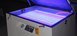
The application of a photoresist layer is a crucial step in the PCB etching process. The resist material is spread evenly over the copper surface and exposed to UV light through a photomask that contains the PCB pattern. This process is known as photolithography and ensures that only the areas of the copper that are exposed to UV light are etched away.
Key steps in photolithography:
- Coating: A thin layer of photoresist is applied to the copper surface.
- Exposure: The photoresist is exposed to UV light through a mask containing the circuit pattern.
- Development: The exposed resist is washed away, leaving the pattern on the copper.
This precise process allows for fine line etching and ensures that the traces are accurately aligned to the design.
UV Exposure and Developing the Resist
The UV exposure step is critical to achieving fine details. The quality of the exposure can affect trace widths and spacing, so it is important to use calibrated exposure units that provide consistent results. After exposure, the development process removes the unwanted resist, allowing the copper to be etched away precisely.
Ensuring Accuracy in Trace Widths and Spacing
In PCB fabrication, maintaining tight tolerances in trace width and spacing is essential for optimal performance. Any variation in trace width or spacing can cause electrical interference, signal degradation, or short circuits. Modern photolithography and etching techniques, combined with computer-aided design (CAD) systems, ensure high accuracy in PCB manufacturing.
Quality Control and Testing
Inspecting Etched PCBs for Defects
Quality control is essential to ensure the reliability and functionality of PCBs. Common defects in etched PCBs include under-etching, over-etching, and unintentional copper residue. To detect these defects, manufacturers use automated optical inspection (AOI) systems, which provide high-resolution imaging of the PCB surface.
Measuring Conductivity and Trace Integrity
Once the PCB is etched, it is tested for conductivity to ensure that the copper traces conduct electricity as intended. This is done through electrical testing, where a small current is passed through the traces to check for any faults or interruptions.
Common Issues Like Under-Etching or Over-Etching
- Under-Etching: This occurs when the etching process does not remove enough copper, leaving traces that are too wide. This can cause circuit malfunctions or poor conductivity.
- Over-Etching: Over-etching occurs when the acid erodes too much copper, causing narrow traces to break or weaken. This can result in signal loss or shorts.
Manufacturers must fine-tune the etching parameters to avoid these issues and ensure the final product meets specifications.
Innovations in PCB Etching Technology
Advances in Laser Etching and Additive Manufacturing
Laser etching and additive manufacturing (3D printing) are emerging technologies that offer new possibilities for PCB fabrication. Laser etching, for example, allows for extremely fine and precise etching, enabling the creation of complex, high-density PCBs with smaller footprints.
Environmental Impact and Sustainable Practices
With increasing concerns over the environmental impact of PCB manufacturing, companies are adopting sustainable practices such as water-based etching solutions and closed-loop recycling systems for etchants. These practices reduce waste and minimize the environmental footprint of the production process.
Future Trends in PCB Fabrication
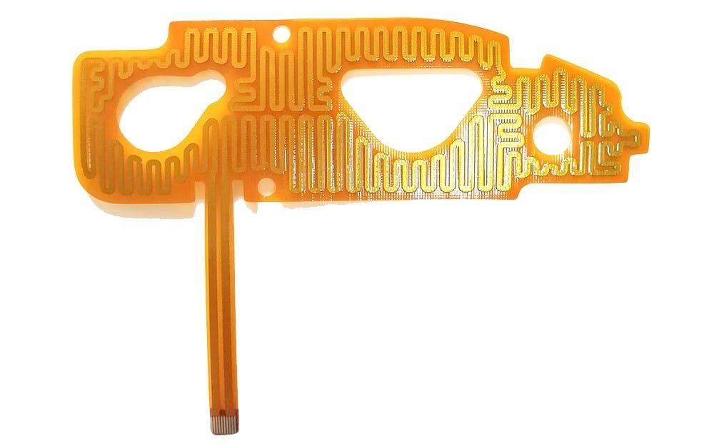
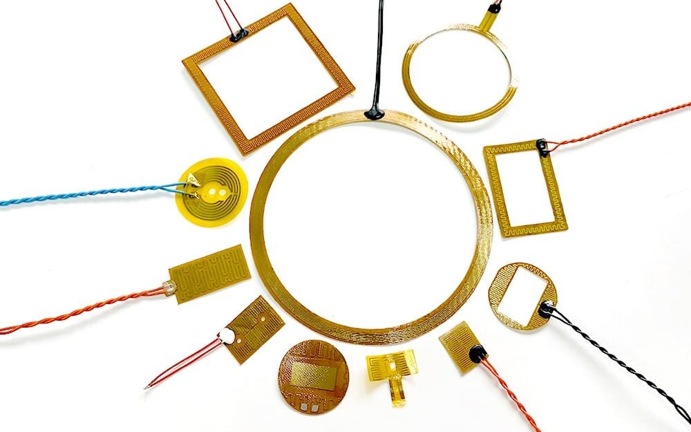
The future of PCB fabrication is leaning toward more integrated and flexible designs, such as flexible PCBs and embedded systems. As electronic devices continue to get smaller and more complex, PCB etching technology will evolve to meet these demands, using innovations like direct-write techniques and advanced nanomaterials.
Chemical etching remains a fundamental technique in the PCB manufacturing process, offering precision and versatility for a wide range of applications. By understanding the role of copper, mastering the etching process, and staying ahead of innovations in the field, engineers and manufacturers can continue to push the boundaries of electronic design. For more in-depth resources on PCB manufacturing, visit industry leaders such as PCBWay for cutting-edge developments.