Why Choosing the Right Process Matters
For product managers and procurement teams, selecting the right manufacturing method for lead frames is crucial for balancing cost, quality, and scalability. Two widely used processes—chemical etching and stamping—offer different benefits. Etching excels in precision and flexibility, while stamping is suited for high-volume production.
This article provides a cost comparison, design flexibility analysis, and real-world ROI case study to help decision-makers choose the most cost-effective lead frame manufacturing solution.

Tooling and Per-Unit Production Costs
One of the key differences between chemical etching and stamping lies in their cost structures.
| Cost Factor | Chemical Etching | Stamping |
|---|---|---|
| Tooling Expenses | Low (Photoresist masks can be quickly modified) | High (Custom stamping dies cost thousands of dollars) |
| Initial Setup Cost | Minimal | Significant investment |
| Per-Unit Cost (Low Volume) | Lower (No expensive tooling required) | Higher (Tooling cost needs to be amortized) |
| Per-Unit Cost (Mass Production) | Higher (Etching speed is slower than stamping) | Lower (Stamping can produce thousands per hour) |
🔹 Key Takeaway: Etching is cost-effective for prototyping and low-to-medium production volumes, while stamping becomes more economical at very high volumes.
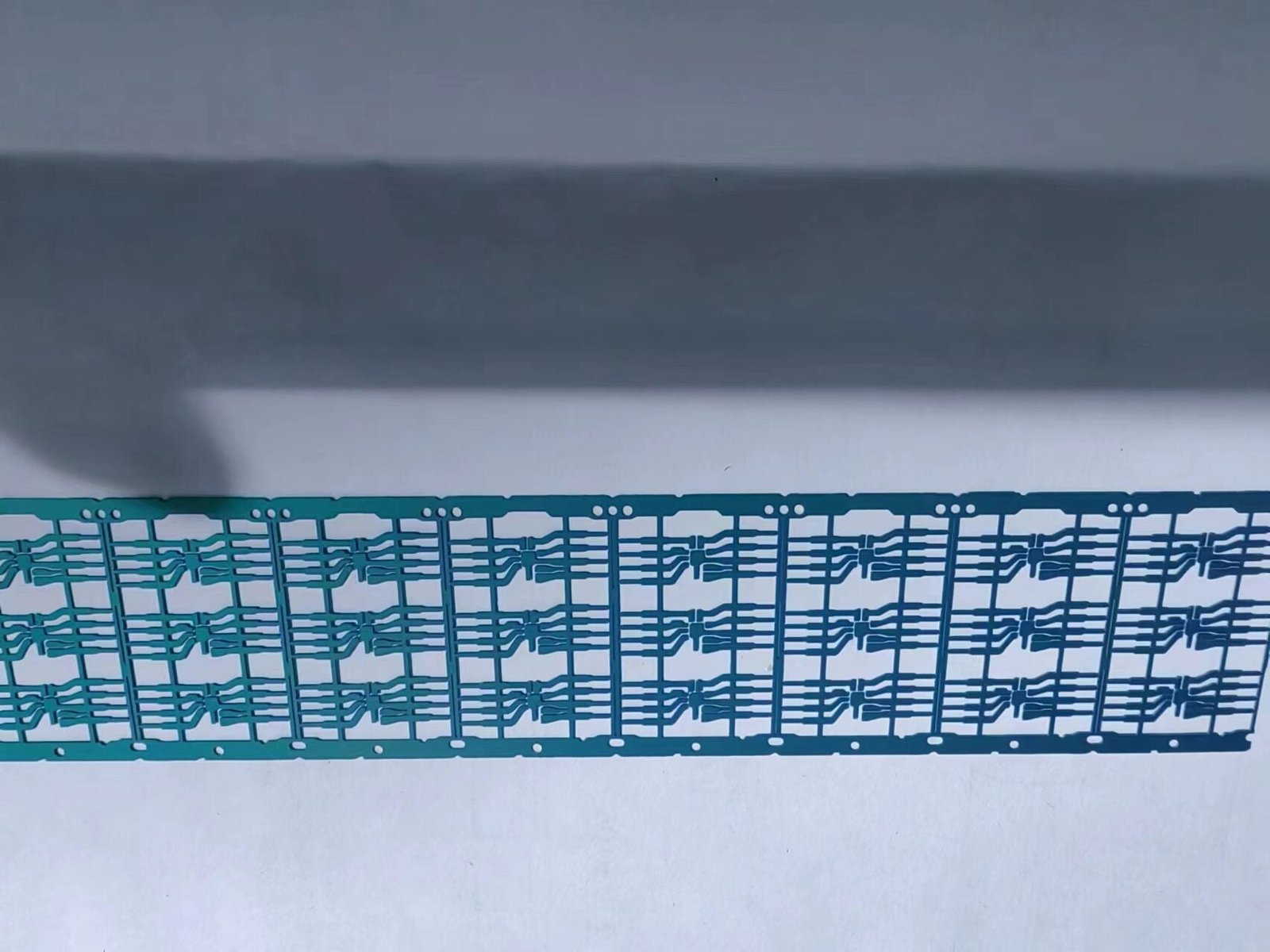
Faster Prototyping and Complex Patterns
In industries like automotive, telecommunications, and medical devices, rapid innovation demands fast turnaround times for lead frame prototyping.
| Factor | Chemical Etching | Stamping |
|---|---|---|
| Lead Time | ~2 weeks | ~8 weeks (for die fabrication) |
| Design Changes | Easy & low-cost (modify mask) | Expensive & slow (requires new die) |
| Feature Precision | ±0.005mm | ±0.02mm |
| Burr-Free Edges | Yes | No (requires post-processing) |
🔹 Key Takeaway: Etching is ideal for lead frames with fine-pitch features (<0.2mm) and quick design iterations. Stamping is better for high-volume, standardized designs.
Industry Example: Semiconductor Prototyping
According to a study by Tech-Etch, etching enables IC designers to test new lead frame designs in weeks rather than months, accelerating time-to-market (source).
Reducing Scrap Rates by 18% in Automotive IC Packaging
A global automotive electronics supplier faced high defect rates using stamped lead frames for their engine control unit (ECU) IC packages.
Challenges:
🔻 Burrs from stamping caused poor solderability.
🔻 Die modifications were expensive and time-consuming.
🔻 Scrap rate exceeded 5%, increasing costs.
Solution:
By switching to chemical etching, the company:
✅ Eliminated burr formation, improving solder joint reliability.
✅ Achieved ±0.005mm precision, enhancing circuit performance.
✅ Reduced scrap rates by 18%, saving thousands in material costs.
📌 Reference: A similar case study from Atotech highlighted how etching reduces lead frame defects, improving overall yield (source).
Ensuring Quality & Cost Efficiency
When choosing a lead frame supplier, procurement teams should evaluate the following:
- Certifications & Quality Standards
- Ensure compliance with IATF 16949 (automotive) and ISO 9001 (general manufacturing).
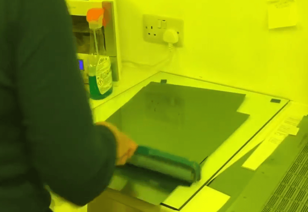
- Etching Process Sustainability
- Recycling etchant baths reduces waste and improves cost efficiency.
- Vendors using regenerative FeCl₃ etching systems minimize chemical consumption.
- DFM (Design for Manufacturability) Support
- Look for vendors offering pre-production simulations to optimize etching parameters.
- Consultation services can help avoid costly redesigns.
✅ Tip: Top-tier suppliers like Xinxin Precision offer DFM optimization and sustainability-focused etching for cost-efficient production.
Miniaturization Driving Demand for <0.2mm Lead Frames
With the rise of 5G, wearables, and IoT devices, lead frames are becoming thinner and more complex.
🔹 Key Trends Shaping the Market:
✔ Fine-Pitch Designs – <50μm traces for high-density IC packaging.
✔ Ultra-Thin Lead Frames – 0.1mm thick or less, reducing package size.
✔ New Materials – Adoption of copper-clad laminates (CCL) and hybrid alloys for better performance.
📌 According to research from SEMI, the demand for high-precision lead frames will grow 12% annually, driven by miniaturization in 5G and automotive electronics (source).
Choosing the Right Solution for Your Needs
Both etching and stamping offer unique advantages depending on cost, production volume, and design complexity.
🔹 When to Choose Etching:
✔ Prototyping and small batches (low tooling costs, fast lead time).
✔ Complex, fine-pitch designs (<0.2mm traces).
✔ Reducing scrap rates and improving plating adhesion.
🔹 When to Choose Stamping:
✔ High-volume production (millions of units per month).
✔ Thicker lead frames where burrs can be managed with post-processing.
✔ Standardized designs with minimal modifications.
For cost-conscious procurement teams, etching offers greater flexibility, lower scrap rates, and easier design iterations, making it a superior choice for next-generation lead frame manufacturing. 🚀