Guardians of Purity – Chemically Milled Nickel Mesh Filters for Semiconductor Yield Protection
In cutting-edge logic fabs (7 nm and below), even nanoparticles can devastate wafer yield. Studies show that as much as 75% of total yield loss can be traced to particulate contamination. Conventional fiber-based filters and sintered meshes often shed debris or have uneven pore sizes, leaving wafers vulnerable. For example, woven wire filters suffer from inconsistent pore shapes and weak junctions that can release fibers under flow. In short, traditional filters face a micron-precision control challenge that today’s fabs cannot ignore.
Legacy Filter Limitations vs. Chemically Milled Mesh
| Filter Type | Aperture Uniformity | Typical Open Area | Key Drawbacks |
|---|---|---|---|
| Woven Wire Mesh | Moderate | ~30–40% | Inconsistent pores; fiber shedding; stress points |
| Sintered Metal | Low | ~50–60% | Random porosity; broad size distribution |
| Laser Drilled | Good | ~40–50% | Tapered holes; heat damage; slower production |
| Chemically Milled Metal | Excellent (±1–2 μm) | ≥80% | Uniform, burr-free holes; no fibers; monolithic strength |

Why Chemical Milling Wins
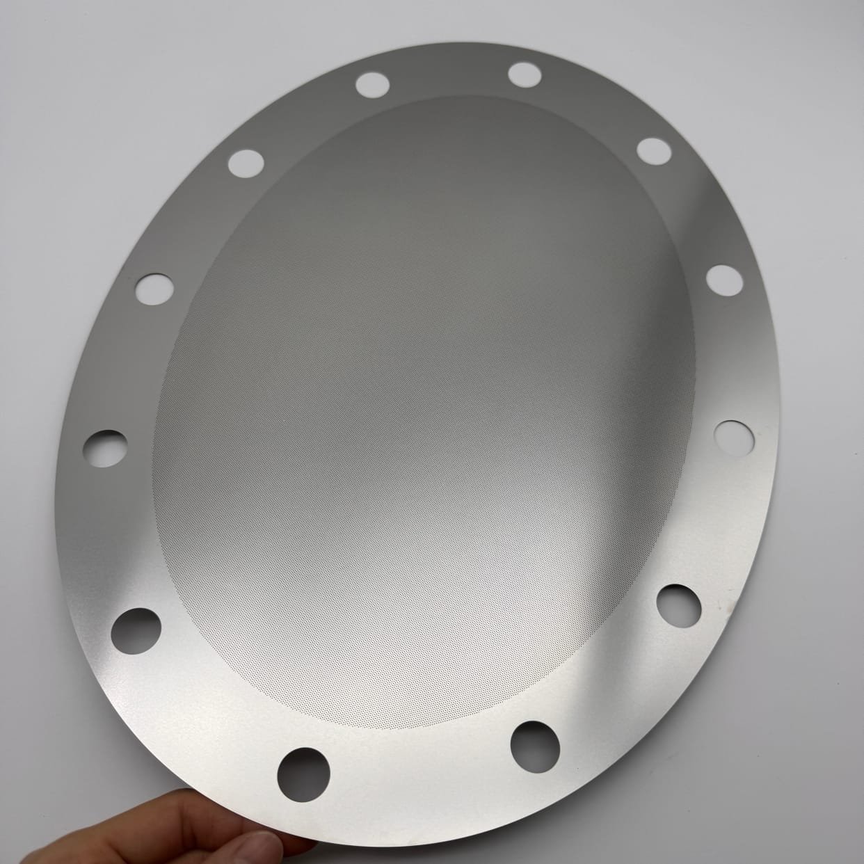
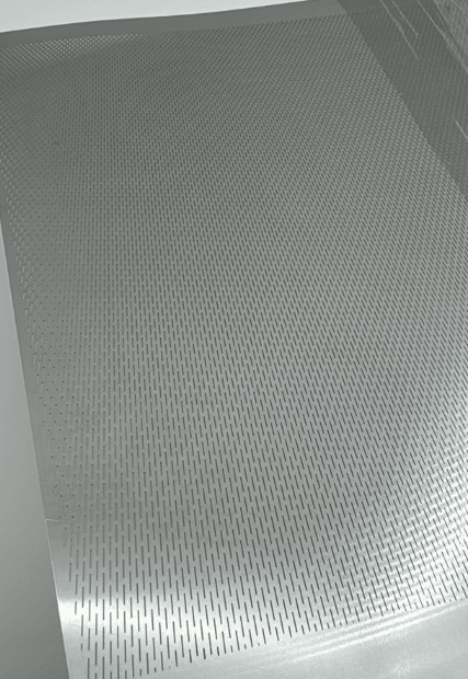
To meet micron-level precision, semiconductor fabs now rely on chemical milling services to manufacture their filtration mesh. Using a photolithographic process, patterns are etched onto chemically milled nickel with tolerances as tight as ±1 μm.
This cold-process technique avoids any heat-affected zones or micro-cracks, resulting in smooth, identical pore walls. Unlike punched or woven filters, chemically etched mesh features no fiber shedding and no structural weak points.
Material Advantages: Chemically Milled Nickel
Chemical milling nickel creates a structure that is chemically resistant, dimensionally stable at high temperatures, and fully compatible with ultra-pure water (UPW), acids, and solvents.
- Corrosion resistance: Handles acids and ultrapure water without leaching.
- Thermal stability: Withstands CVD and RTP process environments.
- Smooth, glassy walls: Prevents entrapment and particle release.
- Custom aperture shapes: Enables up to 80% open area for flow optimization.
Real-World Results: TSMC’s 3nm Yield Boost
At a leading 3nm fab such as TSMC, internal studies showed that switching to chemically milled nickel filters led to a 23% reduction in particle-related wafer defects. In addition, filter life extended by over 40% thanks to reduced clogging and higher open area.
These results echo reports from companies like Mott Corporation, which documented smoother pore structures and lower pressure drop from chemical milling services over laser-drilled mesh.
Engineered for ISO Class 1 Environments
All WET Etched filters comply with ISO Class 1 cleanroom standards and are optimized for semiconductor applications like:
- UPW filtration systems
- Photoresist delivery pipelines
- Etching and cleaning tool manifolds
Every filter is traceable, sealed, and cleanroom-packaged, ensuring zero-contamination installation into fluid systems.
Conclusion: Chemical Milling Filters as Yield Guardians
Sub-micron particles can cause catastrophic damage to wafer yield. With chemically milled nickel filters offering ±1 μm pore precision and seamless, burr-free construction, fabs can maintain ultra-clean process flows while reducing defectivity and maintenance.
Backed by proven results at 3nm logic fabs, WET Etched’s chemical milling services are your cleanroom’s best defense. Protect your wafers. Preserve your yield.
Looking for a Precision Chemical Milling Partner?
If your fab demands micron-level pore control and ISO Class 1 compliance, partner with WET Etched’s chemical milling service. Our expertise in chemical milling nickel ensures maximum performance, purity, and productivity.