Tag Archives: Chemical Etching Copper

Chemical Etching Copper: A Product Manager’s Guide to Applications and Market Trends

Chemical etching copper offers significant potential for product managers to create innovative, high-quality products across various industries. By understanding the applications, cost structures, sourcing considerations, and future trends, you can leverage this versatile process to gain a competitive advantage and drive new product development. Stay ahead of market trends, embrace innovation, and make informed decisions to optimize the use of copper etching in your business.


Overview of Copper Etching Applications

Key Industries: Electronics, Art, Automotive, and Aerospace

Copper etching has diverse applications across multiple industries. Understanding these sectors will help you identify opportunities for product development.

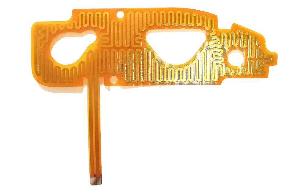
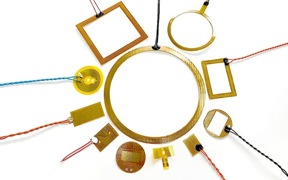
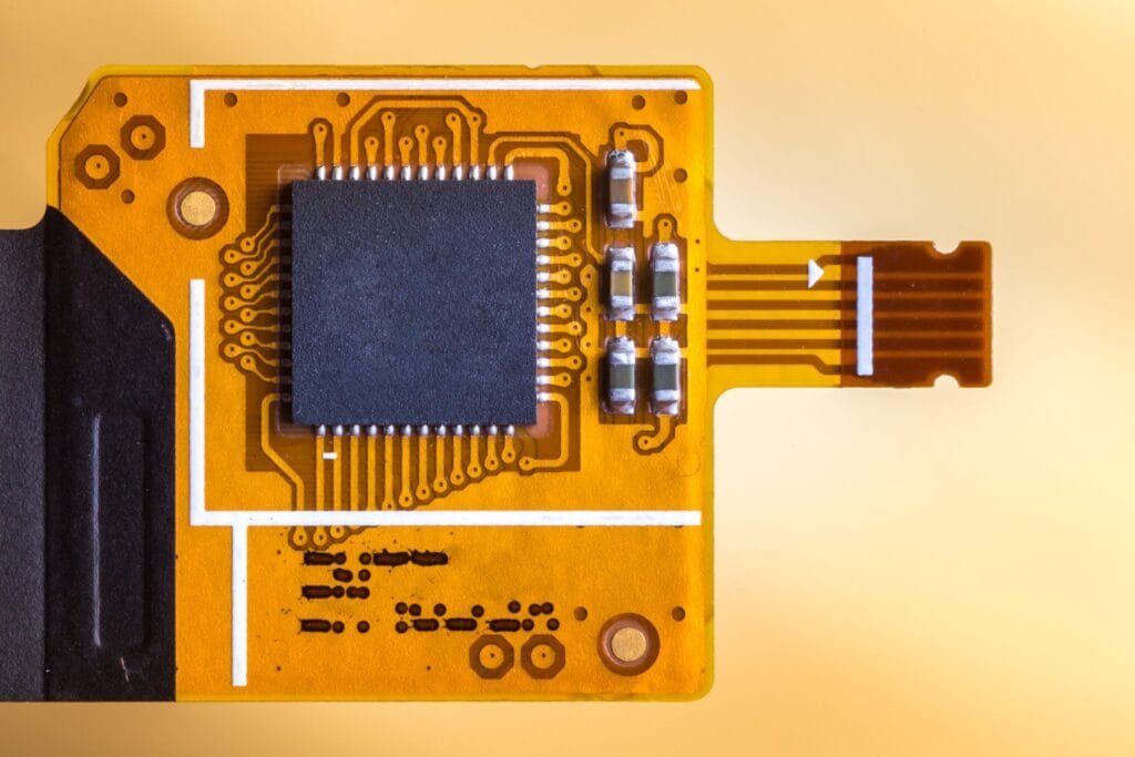
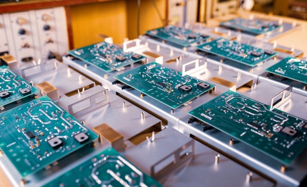
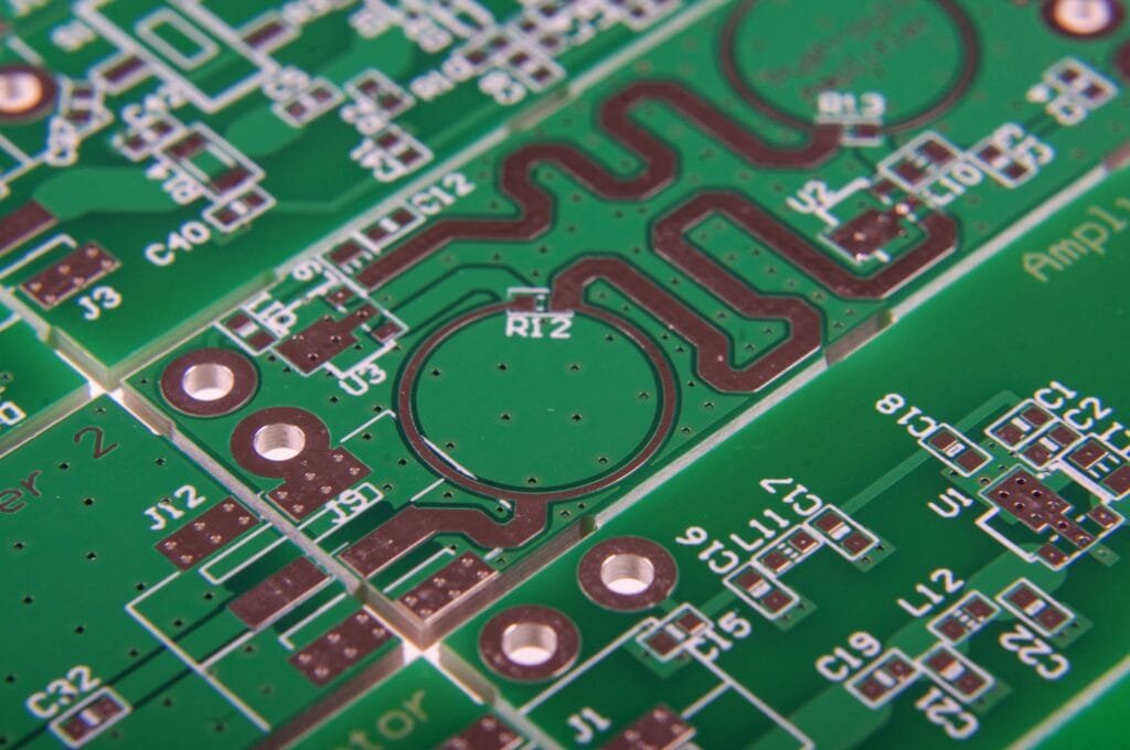
  • Electronics: One of the most significant applications of copper etching is in the production of printed circuit boards (PCBs). The high conductivity, flexibility, and corrosion resistance of copper make it an ideal material for the interconnecting traces found in electronic devices.
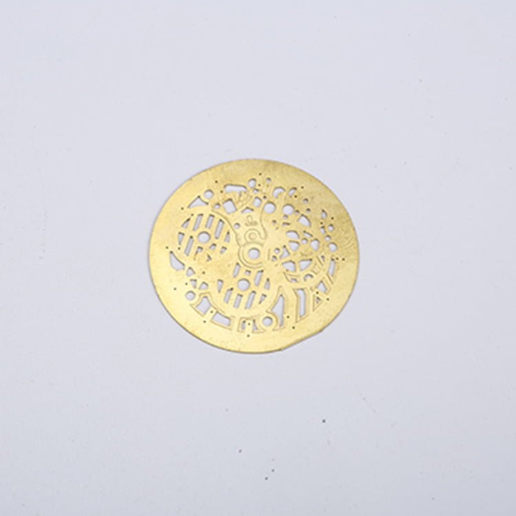
  • Art: Copper etching has long been used by artists to create intricate prints, jewelry, and sculptures. Artists use the etching process to achieve detailed patterns, making it a favorite in fine art and printmaking.
  • Automotive: In automotive manufacturing, copper etching is used for sensors, connectors, and other electronic components that require precision and durability in harsh environments.
  • Aerospace: Aerospace applications rely on copper etching for components such as heat shields, electrical contacts, and connectors. The material’s resistance to high temperatures and its excellent electrical conductivity make it suitable for demanding conditions.

Case Studies of Successful Products Using Etched Copper

  1. Printed Circuit Boards (PCBs): Companies like Intel and Qualcomm rely on precise copper etching for PCB production, allowing for high-density circuits in electronic devices.
  2. Art Prints: Artists such as Rembrandt have used copper etching techniques to produce detailed artworks. Modern artists continue to use this process for limited-edition prints and sculptures.
  3. Automotive Sensors: Companies like Bosch utilize copper etching to create sensors used in vehicles, ensuring precision and reliability.

Market Size and Growth Projections

The copper etching market has seen steady growth due to increased demand for electronics, automotive innovations, and aerospace technologies. According to market research, the global PCB market is projected to reach over $80 billion by 2027, driven by the growing need for smaller, faster, and more efficient electronic devices. This trend will likely propel further advancements in copper etching techniques.

Cost Analysis and ROI

Comparing Etching with Other Manufacturing Methods

When considering copper etching for product manufacturing, comparing the costs to other methods, such as laser cutting, CNC machining, or stamping, is essential for making an informed decision.

MethodAdvantagesDisadvantages
Chemical EtchingHigh precision, cost-effective for complex designsRequires chemical handling, environmental concerns
Laser CuttingHigh speed, clean cuts, minimal material wasteExpensive equipment, limited to certain designs
CNC MachiningIdeal for complex 3D shapes, highly customizableHigher labor and machine costs
StampingBest for high-volume productionLimited design complexity, high setup costs
Comparison of 4 processes

Etching stands out in applications that require intricate details and precision at a lower cost, especially for prototyping and small to medium production runs.

Factors Affecting Cost: Materials, Labor, and Equipment

  • Materials: Copper costs fluctuate based on market demand, quality, and alloy composition. The price of the chemical etchants (e.g., ferric chloride, ammonium persulfate) also affects production costs.
  • Labor: Labor costs for etching vary depending on the complexity of the designs, the number of steps involved, and whether automation is used in the process.
  • Equipment: Investment in etching equipment is relatively low compared to laser or CNC machines, making it a cost-effective option for smaller businesses or prototype development.

Calculating ROI for Etching-Based Products

To calculate the return on investment (ROI) for etching-based products, consider the following factors:

  1. Initial Equipment Investment: Consider the upfront costs of etching equipment and setup.
  2. Production Costs: Account for material costs, labor, and chemicals.
  3. Volume: Etching is particularly cost-effective for medium-volume production runs. As production volume increases, ROI improves due to lower per-unit costs.

Sourcing and Supply Chain Considerations

Finding Reliable Suppliers for Copper and Etching Materials

Sourcing quality copper and etching materials is critical to the success of your production. Here are some factors to consider:

  • Copper Suppliers: Establishing relationships with reliable copper suppliers ensures that you receive consistent quality at competitive prices. Consider global suppliers with strong reputations in the electronics and manufacturing industries.
  • Etching Chemicals: Work with suppliers who provide high-purity etching chemicals and resist materials. It’s essential to ensure that the chemicals meet the required standards for your applications.

Managing Lead Times and Quality Control

Lead time management is essential for maintaining production schedules. Working with suppliers who can deliver on time is crucial to keeping your project on track. Implementing robust quality control systems, including testing materials and inspecting etched products, ensures that the end products meet quality standards and specifications.

Global Market Dynamics and Sourcing Strategies

Global supply chain dynamics play a significant role in sourcing materials. Geopolitical factors, such as trade restrictions or tariffs, can impact copper prices and availability. Diversifying your supplier base and considering local sourcing options may help mitigate risks and stabilize your supply chain.

Innovation and Competitive Advantage

How Etching Can Differentiate Your Product

In a competitive market, differentiation is key. Chemical etching can give your products a competitive edge by enabling intricate designs, reducing manufacturing costs, and offering unique features not easily achieved by other methods.

For example, in the electronics industry, companies that use etching to create compact, high-density PCBs can offer products with more features in smaller devices, a critical factor in consumer electronics.

Collaborating with R&D to Explore New Applications

Work with your research and development (R&D) teams to explore new applications for copper etching. Potential areas for innovation include:

  • Flexible electronics: Copper etching can be used to create thin, flexible PCBs that can be integrated into wearable devices.
  • Sensors and IoT devices: Etching can be employed to manufacture small, precise sensors used in IoT devices and smart technologies.

Protecting Intellectual Property in Etching-Based Designs

As copper etching enables the creation of custom designs, it’s essential to protect intellectual property (IP). Work with legal teams to patent unique designs or manufacturing processes that use copper etching, ensuring your innovations remain exclusive to your business.

Future Trends and Opportunities

Emerging Technologies in Copper Etching

The future of copper etching lies in advancements like laser etching, additive manufacturing, and direct-write technologies. These innovations will offer faster production speeds, finer resolution, and more complex designs. Additionally, the use of nano-inks and 3D printing in combination with copper etching will enable the creation of even more intricate and compact components.

Sustainability and Eco-Friendly Etching Solutions

Environmental considerations are driving demand for sustainable etching solutions. Innovations such as water-based etchants, closed-loop recycling systems for chemicals, and non-toxic alternatives to traditional etchants are reducing the environmental footprint of copper etching. Adopting these eco-friendly practices can enhance your company’s sustainability profile and appeal to environmentally-conscious customers.

Expanding into New Markets and Industries

As technology evolves, copper etching is expanding into new markets such as flexible printed electronics, wearable tech, smart textiles, and automotive electronics. Exploring these new opportunities will allow your business to tap into emerging trends and expand your market reach.

Chemical Etching Copper for PCB Manufacturing: A Technical Deep Dive

Chemical etching is an essential process in the fabrication of printed circuit boards (PCBs). The ability to precisely etch copper patterns onto a board allows for the creation of complex electrical connections that are critical in modern electronic devices. This article explores the technical aspects of using chemical etching for copper PCBs, from material selection to quality control, and examines how the process is optimized for high-precision manufacturing.

The Role of Copper in PCB Fabrication

Why Copper is the Preferred Material for Conductive Layers

Copper is the primary material used in PCB fabrication due to its excellent electrical conductivity, cost-effectiveness, and ease of processing. Copper’s ability to conduct electricity with minimal resistance makes it ideal for forming the conductive traces that interconnect various components on a PCB. In addition, copper has a favorable balance of thermal and mechanical properties that ensures its durability and reliability in electronic devices.

Properties of Copper That Make It Ideal for Etching

The key properties of copper that make it ideal for etching in PCB manufacturing include:

PropertyBenefit for PCB Manufacturing
Electrical ConductivityEnsures efficient transmission of electrical signals.
DuctilityAllows for precise and intricate etching of fine traces.
Corrosion ResistanceEnhances the lifespan of the PCB by preventing degradation.
Thermal ConductivityHelps dissipate heat, reducing the risk of overheating.
Etching properties of copper

Copper’s ductility and excellent corrosion resistance make it particularly well-suited for high-performance and high-reliability electronic devices.

Comparing Copper with Other Conductive Materials

While copper is widely used in PCB manufacturing, other materials like aluminum, gold, and silver are sometimes considered for specific applications. However, copper remains the material of choice due to its balance of performance and cost-efficiency. For example:

MaterialElectrical ConductivityCostCommon Applications
CopperHighLowGeneral-purpose PCBs, consumer electronics
GoldVery HighVery HighHigh-performance electronics, military applications
SilverVery HighHighSpecialized PCBs for high-frequency circuits
AluminumModerateLowLightweight PCBs for certain applications
comparing copper with other conductive materials

Copper’s superior conductivity and lower cost make it the most common choice for mass-produced PCBs.

The Etching Process for PCBs

Step-by-Step Breakdown of the Etching Process

The chemical etching process for PCBs involves several key steps:

  1. Preparing the Copper-Clad Substrate: The process begins with a copper-clad laminate, which is a sheet of base material (typically FR4) coated with a thin layer of copper.
  2. Applying the Photoresist: A photoresist material is applied to the copper surface. This resist will protect the areas of the copper that should remain intact.
  3. Exposure to UV Light: The board is exposed to UV light through a mask or a photomask that contains the PCB pattern. The areas not protected by the photoresist will be etched away.
  4. Development: After exposure, the photoresist is developed, leaving a pattern of resist on the copper.
  5. Etching the Copper: The exposed copper is etched away using a chemical etchant (commonly ferric chloride or ammonium persulfate), leaving the copper traces intact.
  6. Final Cleaning: The remaining photoresist is stripped, leaving behind the finished PCB with copper traces.
It is unbelievable that these devices are needed to manufacture a PCB board.#machine #manufacture
The Etching Process for PCBs

Types of Etchants Used in Industrial Settings

Various etchants are used in the PCB manufacturing process, depending on the desired results and material compatibility. Common etchants include:

EtchantTypeAdvantagesDisadvantages
Ferric ChlorideIron(III) chlorideNon-toxic, widely available, and affordableSlower etching rate compared to other acids
Ammonium PersulfateAmmonium saltFaster etching, good for fine featuresRequires careful handling and disposal
Cupric ChlorideCopper-based etchantProduces smoother etchingMore expensive and requires precise control
Types of Etchants

The choice of etchant depends on the PCB’s specifications, the required etching speed, and the desired level of detail.

Precision and Tolerances in PCB Etching

The precision of PCB etching is critical in ensuring that the electrical traces are both accurate and reliable. In high-end PCBs, the trace width can be as narrow as 2 mils (0.002 inches), with tight tolerances of +/- 10%. To achieve this, manufacturers must control variables such as etchant concentration, temperature, and exposure time to ensure the copper is etched consistently.

Photolithography and Masking Techniques

How Photoresist Layers Are Applied and Patterned

The application of a photoresist layer is a crucial step in the PCB etching process. The resist material is spread evenly over the copper surface and exposed to UV light through a photomask that contains the PCB pattern. This process is known as photolithography and ensures that only the areas of the copper that are exposed to UV light are etched away.

Key steps in photolithography:

  1. Coating: A thin layer of photoresist is applied to the copper surface.
  2. Exposure: The photoresist is exposed to UV light through a mask containing the circuit pattern.
  3. Development: The exposed resist is washed away, leaving the pattern on the copper.

This precise process allows for fine line etching and ensures that the traces are accurately aligned to the design.

UV Exposure and Developing the Resist

The UV exposure step is critical to achieving fine details. The quality of the exposure can affect trace widths and spacing, so it is important to use calibrated exposure units that provide consistent results. After exposure, the development process removes the unwanted resist, allowing the copper to be etched away precisely.

Ensuring Accuracy in Trace Widths and Spacing

In PCB fabrication, maintaining tight tolerances in trace width and spacing is essential for optimal performance. Any variation in trace width or spacing can cause electrical interference, signal degradation, or short circuits. Modern photolithography and etching techniques, combined with computer-aided design (CAD) systems, ensure high accuracy in PCB manufacturing.

Quality Control and Testing

Inspecting Etched PCBs for Defects

Quality control is essential to ensure the reliability and functionality of PCBs. Common defects in etched PCBs include under-etching, over-etching, and unintentional copper residue. To detect these defects, manufacturers use automated optical inspection (AOI) systems, which provide high-resolution imaging of the PCB surface.

Measuring Conductivity and Trace Integrity

Once the PCB is etched, it is tested for conductivity to ensure that the copper traces conduct electricity as intended. This is done through electrical testing, where a small current is passed through the traces to check for any faults or interruptions.

Common Issues Like Under-Etching or Over-Etching

  • Under-Etching: This occurs when the etching process does not remove enough copper, leaving traces that are too wide. This can cause circuit malfunctions or poor conductivity.
  • Over-Etching: Over-etching occurs when the acid erodes too much copper, causing narrow traces to break or weaken. This can result in signal loss or shorts.

Manufacturers must fine-tune the etching parameters to avoid these issues and ensure the final product meets specifications.

Innovations in PCB Etching Technology

Advances in Laser Etching and Additive Manufacturing

Laser etching and additive manufacturing (3D printing) are emerging technologies that offer new possibilities for PCB fabrication. Laser etching, for example, allows for extremely fine and precise etching, enabling the creation of complex, high-density PCBs with smaller footprints.

Environmental Impact and Sustainable Practices

With increasing concerns over the environmental impact of PCB manufacturing, companies are adopting sustainable practices such as water-based etching solutions and closed-loop recycling systems for etchants. These practices reduce waste and minimize the environmental footprint of the production process.

Future Trends in PCB Fabrication

The future of PCB fabrication is leaning toward more integrated and flexible designs, such as flexible PCBs and embedded systems. As electronic devices continue to get smaller and more complex, PCB etching technology will evolve to meet these demands, using innovations like direct-write techniques and advanced nanomaterials.


Chemical etching remains a fundamental technique in the PCB manufacturing process, offering precision and versatility for a wide range of applications. By understanding the role of copper, mastering the etching process, and staying ahead of innovations in the field, engineers and manufacturers can continue to push the boundaries of electronic design. For more in-depth resources on PCB manufacturing, visit industry leaders such as PCBWay for cutting-edge developments.

The Art and Science of Chemical Etching Copper: A Beginner’s Guide

Chemical etching copper is a fascinating process that combines artistic creativity with scientific precision. Whether you’re a DIY enthusiast or just curious about how intricate designs are made on metal, this beginner’s guide will help you understand the process, history, materials, and techniques behind copper etching. Let’s explore how you can start your own etching projects at home and make beautiful, personalized pieces.

What is Chemical Etching?

Definition and Overview of the Process

Chemical etching, also known as acid etching, is a technique used to create patterns or designs on a surface by applying a corrosive substance (usually an acid) to the metal. When applied to copper, the acid erodes the unprotected areas of the metal, leaving behind a clean, etched design. This process allows for extremely detailed and intricate designs, which makes it ideal for art, industrial applications, and custom projects.

Chemical Etching Samples

Historical Context

The technique of chemical etching dates back to the early 16th century when William Blake, the famous British poet and artist, used it to create his illuminated books. Throughout history, artists and craftsmen have used etching to create detailed images on metal plates, and the process evolved into a significant artistic method. Today, chemical etching is still used in modern art, electronics (such as PCB etching), and even jewelry-making.

Discovering William Blake's Innovative Printing Process

Why Copper?

Copper is a highly versatile material, making it an excellent choice for etching. Some of its key properties include:

PropertyBenefits for Etching Copper
DuctilityCopper is flexible and easy to manipulate.
ConductivityCopper’s electrical properties are ideal for certain applications (e.g., PCB etching).
Corrosion ResistanceCopper resists corrosion, ensuring long-lasting etchings.
Smooth SurfaceThe natural smoothness of copper makes it an ideal canvas for intricate designs.
Characteristics of copper

These attributes make copper a favorite among artists, engineers, and hobbyists alike.

Materials and Tools You’ll Need

To begin copper etching at home, you will need a few essential materials and tools. Here’s a list of what you’ll need:

Material/ToolPurpose
Copper SheetsThe base material for your etching project. Available in various thicknesses and sizes.
Acid-Resistant VarnishTo protect areas of copper that you don’t want to etch.
Nitric Acid or Ferric ChlorideThe etching solution that will erode the copper. (Note: Always follow safety instructions.)
BrushesFor applying varnish and ink evenly.
Steel Wool or SandpaperFor cleaning the copper before applying varnish.
Protective GearGloves, goggles, and a mask to protect from the corrosive acids.
Tools Needed for Etching Copper

Safety Precautions

When working with chemicals like nitric acid, it’s crucial to prioritize safety. Always wear gloves, goggles, and a mask when handling acids. Work in a well-ventilated area, and follow all manufacturer instructions on the chemical containers. Be sure to have a neutralizing agent (such as baking soda) handy in case of spills.

You can find many of these materials on platforms like Amazon or AliExpress, where you’ll find etching kits suitable for beginners.

Step-by-Step Etching Process

Preparing the Copper Sheet

  1. Clean the Copper: Use steel wool or sandpaper to gently scrub the copper sheet, removing any dirt, oils, or oxidation. This ensures that the varnish will adhere properly.
  2. Apply Acid-Resistant Varnish: Use a brush to apply an acid-resistant varnish or resist to the copper sheet. This will protect the areas of the copper that you want to remain untouched by the acid.
  3. Create Your Design: If you’re working with a pre-made design, print it out in reverse and transfer it onto the varnished copper sheet. If you’re drawing by hand, make sure to work in reverse as well, as the etching process will flip the design.

The Acid Bath

  1. Prepare the Etching Solution: Mix your acid (either nitric acid or ferric chloride) according to the instructions provided. Ensure you’re in a well-ventilated area and using appropriate safety gear.
  2. Submerge the Copper Sheet: Carefully place the copper sheet in the acid bath. The acid will begin to eat away the exposed copper, creating the design you’ve applied.
  3. Timing: Keep a close eye on the copper as it etches. Depending on the depth of the etch and the acid used, it may take anywhere from 30 minutes to a few hours.
  4. Neutralize the Acid: Once you’ve achieved your desired etching depth, carefully remove the copper and neutralize the acid with baking soda or water.

Printing Your Design

Once your design is etched into the copper, it’s time to transfer it onto paper or fabric.

  1. Inking the Etched Plate: Apply ink to the etched copper plate using a soft, even layer. Make sure the ink gets into all the etched areas.
  2. Using a Press: If you have access to a printing press, use it to transfer the ink from the copper plate to your chosen material. For DIY methods, you can use a baren or even a rolling pin to apply pressure and transfer the design.

Troubleshooting Common Issues

  • Ink Smudges: If the ink smears, try reducing the amount of ink you apply to the plate or let it dry a bit longer before pressing.
  • Uneven Etching: If the acid didn’t etch evenly, it could be due to uneven varnish application. Ensure your resist is applied smoothly.

Creative Applications of Copper Etching

Artistic Projects

Copper etching is a fantastic way to create personalized art, from custom prints to jewelry. Artists like Rembrandt used copper etching as their preferred method for creating intricate prints, while modern artists experiment with new designs and techniques.

You can create beautiful etched artwork, or even make custom jewelry like etched pendants or bracelets. Try experimenting with different acid strengths and varnish techniques for varied results.

Practical Uses

  • Circuit Boards: Copper etching is widely used in the manufacturing of printed circuit boards (PCBs) for electronics. The same process used in art can be scaled up for industrial use.
  • Decorative Items: Use copper etching to create custom home decor, such as etched copper plates, coasters, or even furniture embellishments.

Inspiring Examples

Many modern artists, like David Hockney, have incorporated copper etching into their artistic processes, blending modern techniques with traditional methods.

For more inspiration and to see how artists have been using chemical etching in their work, check out this blog post on copper etching.