Chemical Machining
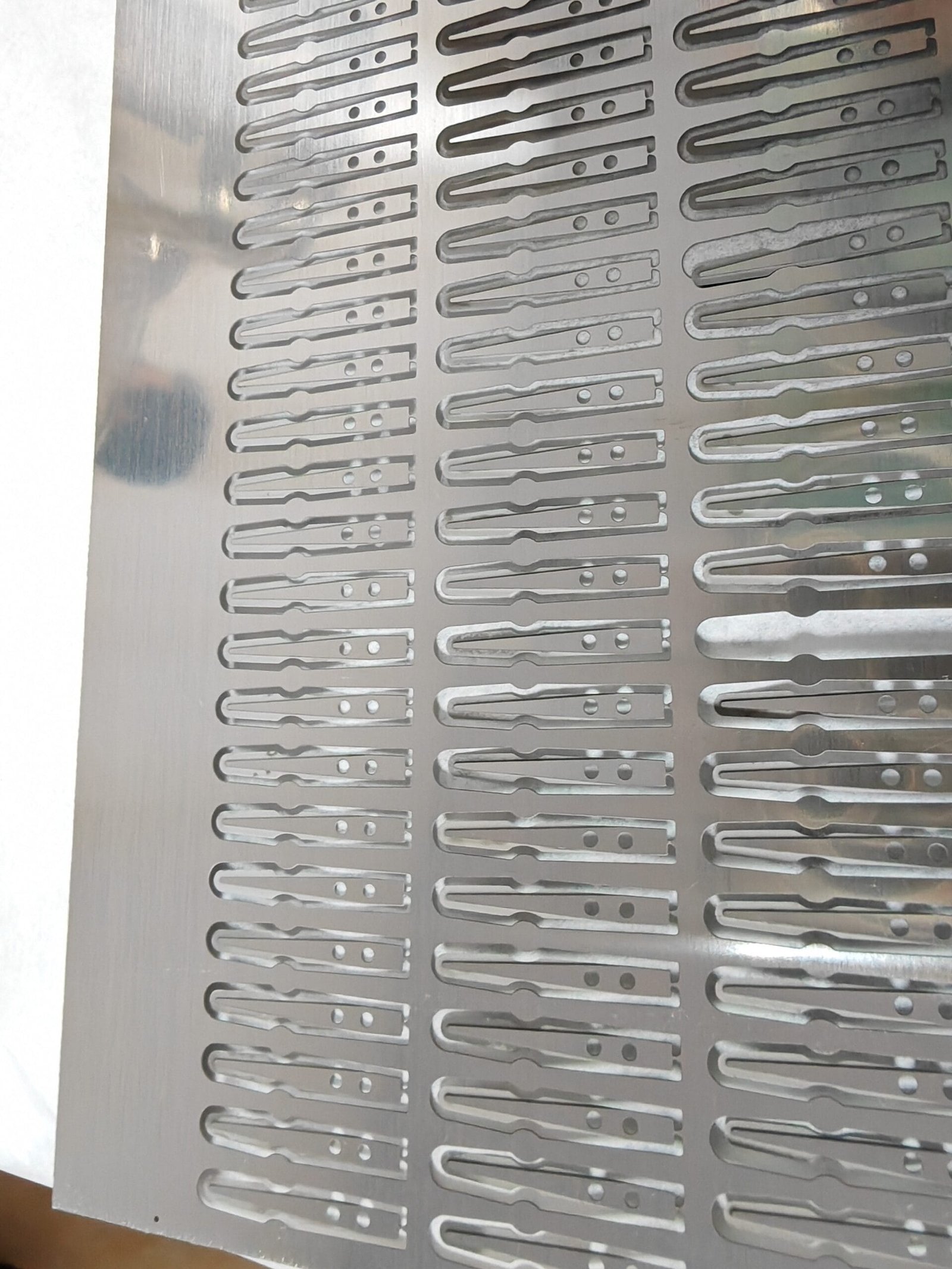
Chemical Etching Machine for Micro Surgical Blades, Crescent Blades, and Keratomes Manufacturing
- By wetetched.com
- 1 Apr 2026
- 0
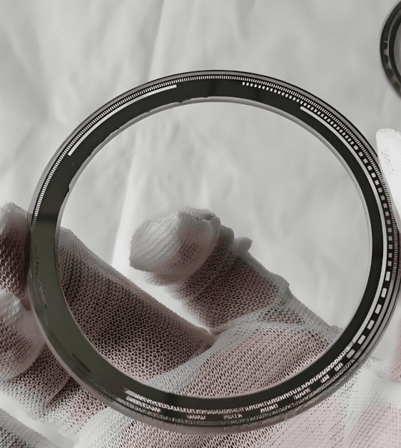
Optical Encoder Accuracy: The Science Behind Chemically Milled Gratings
- By wetetched.com
- 9 Jul 2025
- 0
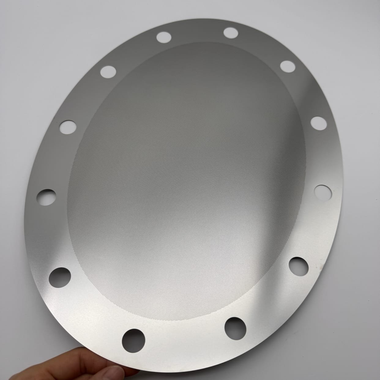
Guardians of Purity: Micron-Perfect Nickel Mesh Filters for Semiconductor Fabs
- By wetetched.com
- 9 Jul 2025
- 0
Precision Gratings Explained | Optical Encoder Accuracy & Chemically Milled Gratings
- By wetetched.com
- 9 Jul 2025
- 0
Maximize Encoder Lifespan: Corrosion-Resistant Stainless Steel Gratings via Chemical Milling
- By wetetched.com
- 9 Jul 2025
- 0
Scaling Advanced Chemical Etching Strategies for High-Volume Production
- By wetetched.com
- 22 Apr 2025
- 0

Why Chemical Etching in Everyday Tech: The Invisible Innovation
- By wetetched.com
- 22 Apr 2025
- 0
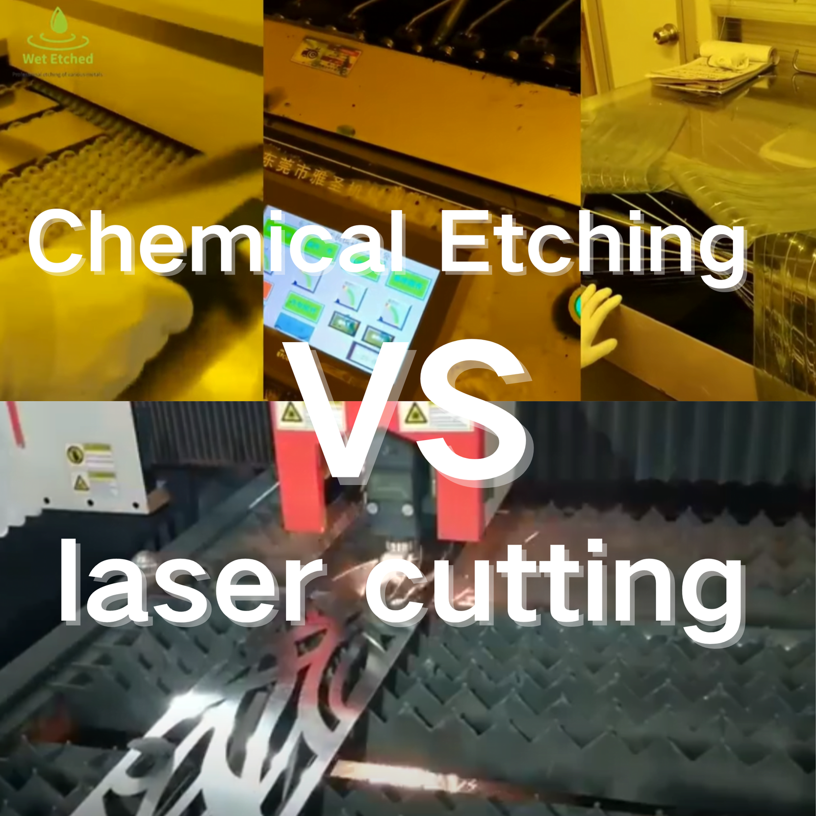
Why Advanced Chemical Etching Beats Laser Cutting for Complex Metal Parts
- By wetetched.com
- 22 Apr 2025
- 0
Why Top Automotive Brands Choose PCM for Stainless Steel Microcomponents
- By wetetched.com
- 10 Apr 2025
- 0