All posts by wetetched.com

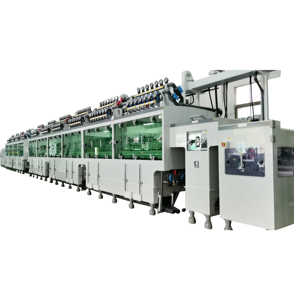
Chemical Etching Aluminum: Detailed Steps

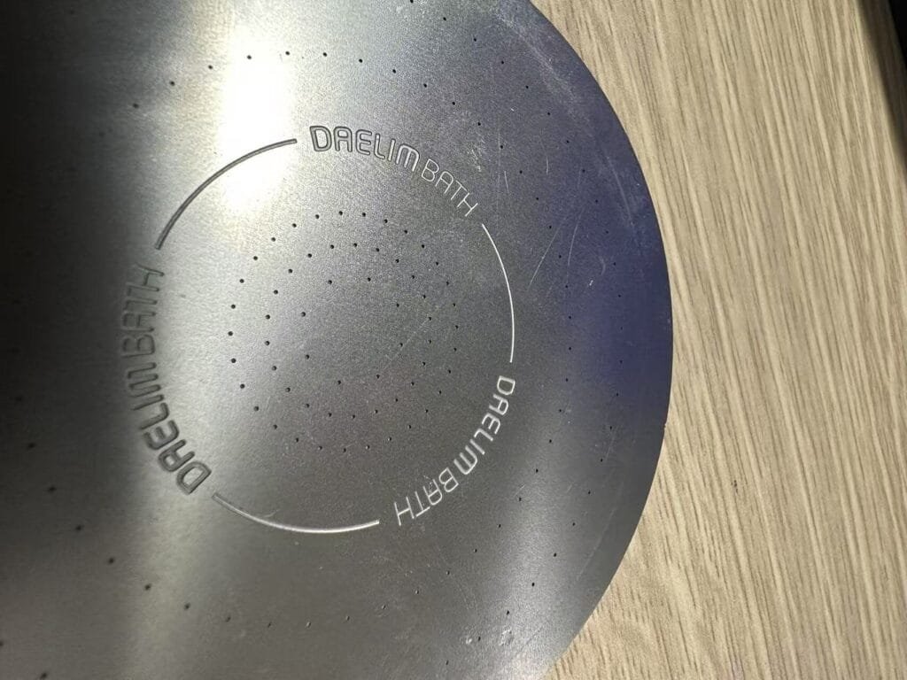
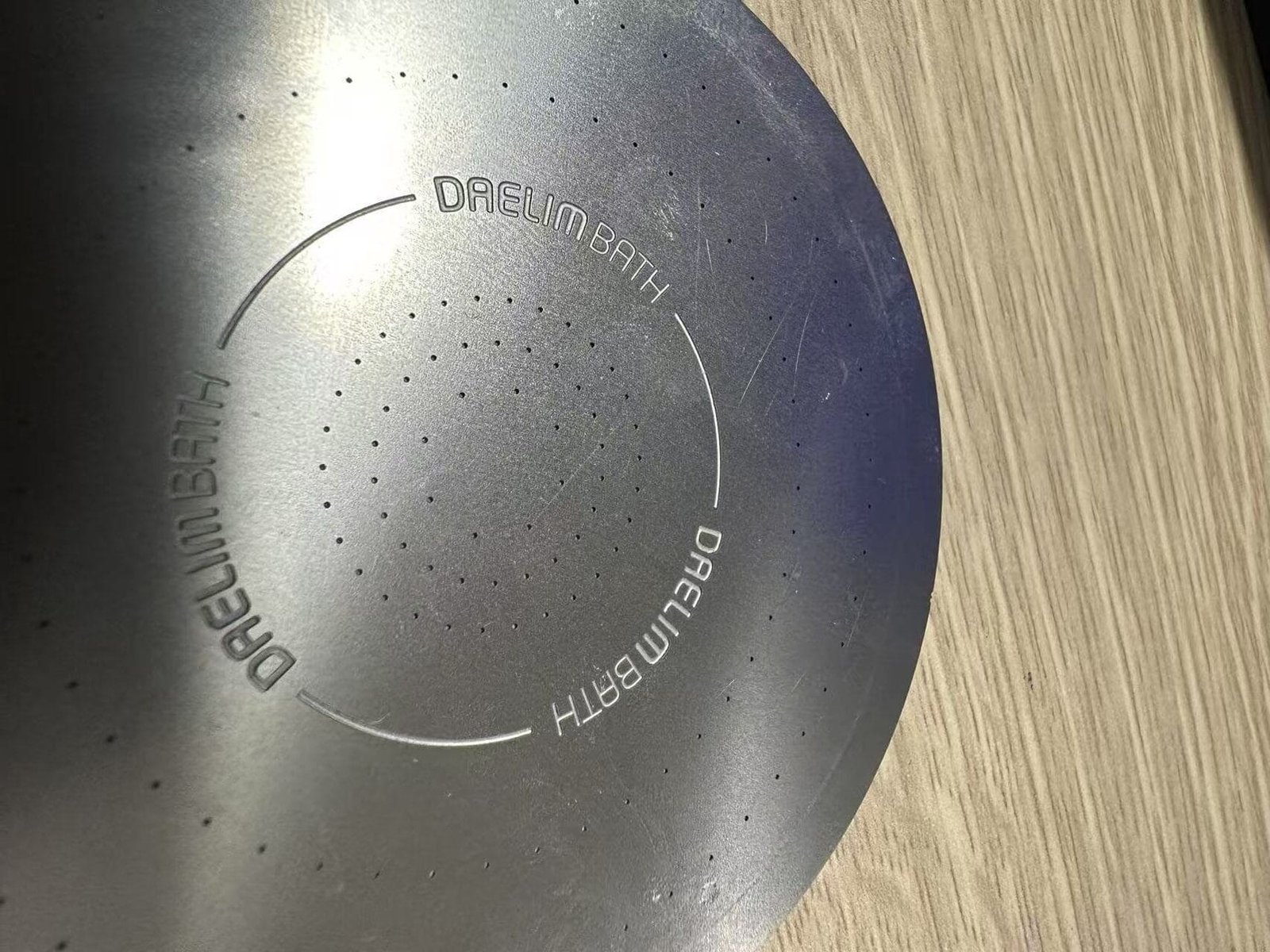
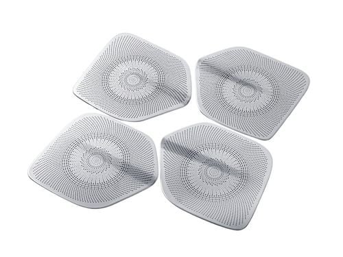
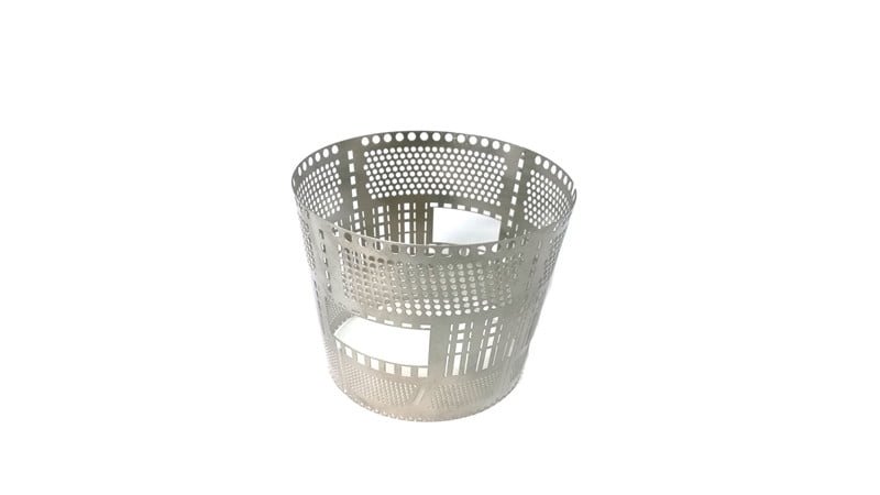
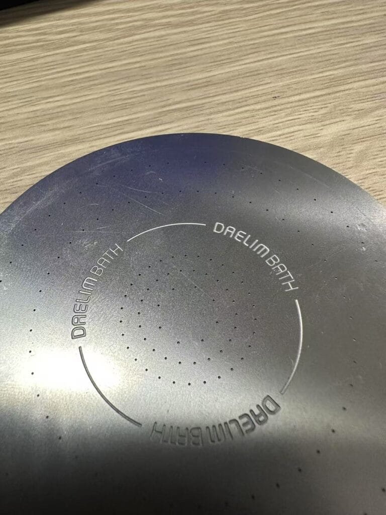
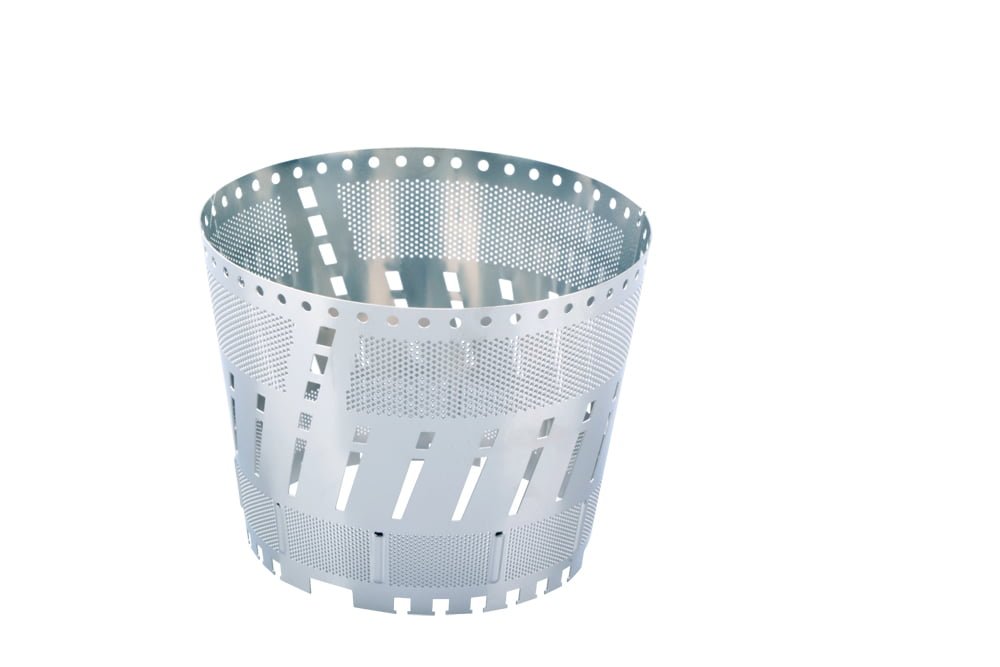
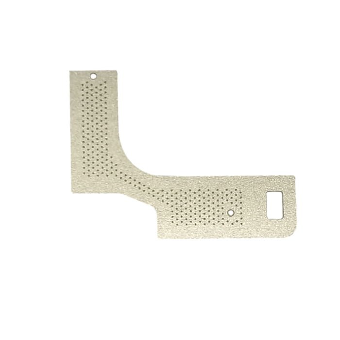
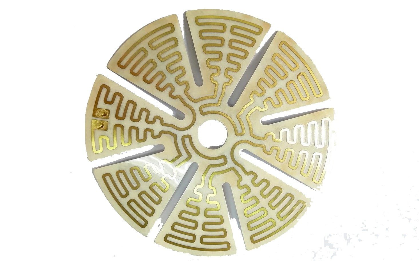
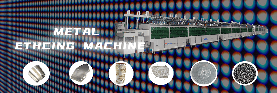
Chemical Etching Samples

1. Raw Material Selection

The process begins with the selection of high-quality aluminum. The choice of aluminum alloy depends on the specific application and desired properties of the final product. Commonly used alloys include 6061 and 7075 due to their excellent mechanical properties and corrosion resistance.

2. Cleaning Line

Before any chemical processing, the aluminum must be thoroughly cleaned to remove any contaminants that can interfere with etching.

Steps:

  • Water Rinse: Use deionized (DI) water to rinse the aluminum sheets. DI water prevents impurities from affecting subsequent steps.
  • Cleaning Solution: Immerse the aluminum in a cleaning solution, typically an alkaline cleaner, to remove oils, grease, and other contaminants.
  • Rinse: Rinse again with DI water to remove any residues of the cleaning solution.
  • Drying: Use hot air dryers to completely dry the aluminum sheets.

Water Quality Recommendation: Use deionized water with a resistivity of at least 18 MΩ·cm to ensure no ionic contamination.

3. Painting and Drying Line

After cleaning, a photoresist is applied to the aluminum surface. The photoresist will protect areas that should not be etched.

Steps:

  • Application: Apply a uniform coat of liquid photoresist or dry film photoresist using a roller or spray system.
  • Pre-drying: Partially dry the photoresist to remove solvents without curing it, typically in a convection oven.
  • Final Drying: Cure the photoresist in a controlled environment. This usually involves a conveyorized oven with precise temperature control.

Temperature Control:

  • Pre-drying: 100-120°C for 1-2 minutes.
  • Final Drying: 150-180°C for 5-10 minutes, depending on the specific resist material.

4. Exposure Line

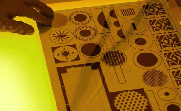
In this step, the photoresist-coated aluminum is exposed to UV light to create the desired pattern. The choice between LED and Laser Direct Imaging (LDI) exposure depends on the required precision and complexity.

LED Exposure:

  • Process: The aluminum is placed in an exposure unit, and a photomask is aligned over it. UV LEDs expose the photoresist through the photomask.
  • Workflow: Align photomask → Expose with UV LED → Move to developing line.
  • Advantages: Cost-effective, suitable for less complex patterns.

LDI Exposure:

  • Process: Directly writes the pattern onto the photoresist using a laser, eliminating the need for a photomask.
  • Workflow: Program design into LDI system → Expose photoresist with laser → Move to developing line.
  • Advantages: High precision, ideal for complex and high-resolution patterns.

5. Developing Line

After exposure, the photoresist needs to be developed to reveal the pattern that will be etched.

Steps:

  • Developer Solution: Immerse the exposed aluminum in a developer solution, typically a diluted alkaline solution.
  • Rinse: Rinse with DI water to stop the development process and remove all developer residues.
  • Drying: Dry the aluminum using hot air dryers.

Why Developing is Necessary: Developing removes the exposed (or unexposed, depending on the type of resist) areas of the photoresist, creating the precise pattern needed for etching.

6. Aluminum Etching Line

The developed aluminum is now ready for etching, which removes the unprotected areas of the metal.

Using Copper Sulfate Etchant:

Steps:

  • Etchant Preparation: Prepare a copper sulfate etchant solution. A common recipe is:
    • Copper sulfate (CuSO₄): 150-200 g/L
    • Sulfuric acid (H₂SO₄): 50-100 g/L
    • Temperature: 45-60°C
  • Etching Process: Immerse the aluminum in the etchant solution. The unprotected aluminum areas will be dissolved, leaving the desired pattern.
  • Agitation: Use mild agitation to ensure even etching.
  • Duration: Etching time depends on the desired depth and pattern complexity, typically 5-15 minutes.
  • Rinse: Rinse thoroughly with DI water to remove etchant residues.

Parameters:

  • Temperature: Maintain at 50-55°C for optimal etching speed and precision.
  • Proportion: Ensure the etchant solution is regularly monitored and replenished to maintain effectiveness.

7. Stripping Line

After etching, the remaining photoresist must be stripped away to reveal the final metal pattern.

Steps:

  • Stripping Solution: Use a photoresist stripper solution, often an alkaline or solvent-based solution.
  • Immersion: Immerse the etched aluminum in the stripping solution until all photoresist is removed.
  • Rinse: Rinse with DI water to remove any stripper residues.
  • Final Drying: Dry the aluminum using hot air dryers.

Details:

  • Stripper Solution Temperature: Typically 40-60°C.
  • Immersion Time: 5-10 minutes, depending on the resist thickness and type.

If you need a OEM factory to realize your project, please do not hesitate to contact us.

Wet Chemical Etching Company is a leading provider of wet chemical etching services, dedicated to delivering high-quality and precise etching solutions for the semiconductor, microelectronics, and precision manufacturing industries. Equipped with advanced technology and state-of-the-art equipment, our company can handle various materials and complex pattern requirements. Our professional team has extensive experience and expertise, ensuring that every project is delivered on time and meets the highest quality standards. Whether for prototype development or large-scale production, Wet Chemical Etching Company is committed to customer satisfaction, offering customized and efficient services to help your products succeed in the market.

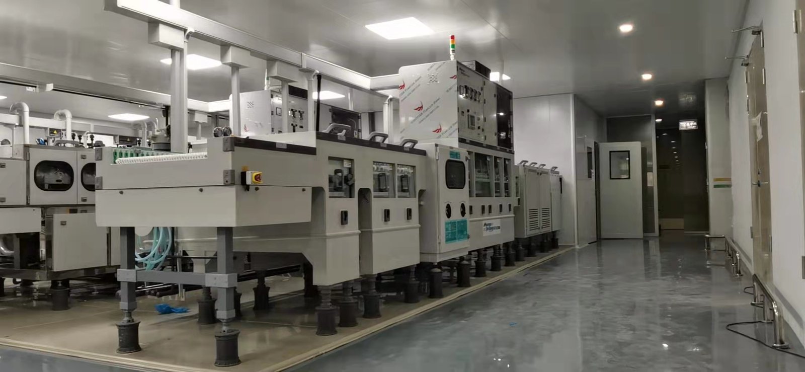
    WET Aluminum etching

    Wet Metal Etching Production workshop-  Shenzhen Xinxin Precision Equipment Co., Ltd.
    WET Aluminum etching production

    The Essential Role of Fine Tungsten Probes in Surgical Instruments

    In the realm of surgical instruments, precision is paramount. Whether it’s general surgery, plastic surgery, or specialized procedures, the accuracy and reliability of surgical tools can significantly impact patient outcomes. One crucial component that has emerged as indispensable in this context is the fine tungsten probe. This blog explores the significance of tungsten probes in surgical instruments and their applications across various medical fields, emphasizing the customization and precision they bring to the table.

    Tungsten probes are known for their exceptional strength and durability, making them ideal for delicate surgical procedures that require precise manipulation. The fine tip of a tungsten probe allows surgeons to navigate through tissues with ease, minimizing trauma and reducing the risk of complications. Additionally, the high thermal conductivity of tungsten ensures that the probe remains cool during use, preventing tissue damage from heat.

    In plastic surgery, tungsten probes are used for tasks such as sculpting and shaping tissues with precision. The ability to customize the shape and size of tungsten probes allows surgeons to achieve the desired aesthetic outcomes with accuracy. In neurosurgery, tungsten probes are utilized for delicate procedures such as tumor resection and nerve repair, where precision is critical to preserving neurological function.

    Overall, the versatility and reliability of tungsten probes make them an essential tool in the arsenal of surgical instruments. Their ability to provide customization, precision, and durability sets them apart in the field of medicine, where every millimeter and every movement counts towards a successful outcome for the patient.

    Understanding Fine Tungsten Probes

    Fine tungsten probes are known for their exceptional hardness, high melting point, and excellent electrical conductivity. These properties make them ideal for use in a variety of high-precision applications, including surgical instruments. Here, we’ll delve into the key parameters of tungsten probes and how they enhance surgical tools:

    • Probe Tip Diameter: Ranges from 0.001 to 0.020 inches, allowing for delicate and precise probing essential in surgery.
    • Tip Radius: Typically between 0.0005 and 0.005 inches, crucial for detailed work on small structures.
    • Taper Length: Varies from 0.010 to 0.200 inches, providing flexibility in different surgical applications.
    • Overall Length: Spanning 0.050 to 1.000 inches, tailored to specific surgical needs.
    • Shaft Diameter: From 0.005 to 0.050 inches, ensuring a sturdy yet manageable tool.
    • Coating: Optional coatings can enhance properties such as biocompatibility and durability.

    Applications in Surgical Instruments

    General Surgery

    In general surgery, precision tools are necessary for a variety of procedures. Fine tungsten probes assist in delicate tissue manipulation and provide the accuracy needed for incisions and sutures. Instruments like surgical scissors and forceps benefit from the integration of tungsten probes for their fine tips and robust construction.

    Plastic Surgery

    Plastic surgery often involves working with delicate structures and soft tissues. Tungsten probes, with their fine tips and customizable features, are ideal for these procedures. They help in tasks requiring meticulous detail, such as reconstructive surgery or cosmetic enhancements.

    Controlling Bleeding

    Hemostats and other clamping instruments play a critical role in controlling bleeding during surgery. Tungsten probes enhance the efficacy of these tools with their precise gripping and clamping capabilities. The fine tips and serrated jaws of forceps such as Adson forceps and hemostats benefit from tungsten probes, offering better control and reduced tissue trauma.

    Types of Surgical Instruments Enhanced by Tungsten Probes

    Forceps

    Forceps are vital in various surgical procedures for holding, grasping, and manipulating tissues. Tungsten probes enhance the performance of different types of forceps, including tissue forceps, hemostats, and Adson forceps, by providing fine tips and improved grip.

    Scissors

    Surgical scissors, like Mayo scissors, require sharp and precise edges. Tungsten probes contribute to the durability and sharpness of these scissors, ensuring clean cuts and improved surgical outcomes.

    Clamps

    Surgical clamps, used to control blood flow and secure tissues, benefit from tungsten probes’ strength and precision. The ratchet mechanism in clamps becomes more effective with the integration of tungsten probes, offering reliable performance during operations.

    Customization and Innovation

    Manufacturers like WET specialize in batch customization of fine tungsten probes, catering to the specific needs of the medical field. This customization ensures that each probe meets the exacting standards required for various surgical tools, from forceps and scissors to specialized instruments for plastic and general surgery.

    Conclusion

    In the world of surgical instruments, every micron matters. Fine tungsten probes, with their precision and customizable features, are transforming the landscape of surgical tools. They play a crucial role in enhancing the performance and reliability of various surgical instruments, from general surgery to highly specialized procedures. As innovation in precision engineering continues, the importance of fine tungsten probes in the medical field will undoubtedly grow, driving advancements and improving patient care.

    For more information on tungsten probes and their applications in surgical instruments, visit WET’s website or contact their team for customized solutions tailored to your surgical needs.

    With the increasing demand for more precise and reliable surgical instruments, the use of fine tungsten probes is becoming more prevalent in the medical field. These probes offer unparalleled accuracy and durability, making them essential tools for surgeons performing delicate procedures. By partnering with a reputable manufacturer like WET, healthcare professionals can access high-quality tungsten probes that are tailored to their specific requirements. As technology continues to advance, the role of fine tungsten probes in surgical instruments will only become more significant, ultimately leading to better outcomes for patients. Visit WET’s website today to learn more about how tungsten probes can elevate the performance of surgical tools and improve patient care.

    The Chemical Etching Titanium Process: Precision and Innovation with WET Etched

    The chemical etching process for titanium creates precision components by selectively removing metal through a photoresist mask. This advanced technique offers numerous advantages over conventional sheet metalworking, including the ability to produce parts without degrading material properties, as no force or heat is used during processing. It also allows for almost limitless part complexity, with component features machined simultaneously using etchant chemistries.

    Table of Contents

    What is Chemical Etching Titanium and How Does It Work?

    Chemical etching titanium is a metalworking process that utilizes specialized corrosive chemicals to etch complex and precise components from titanium. This process is highly favored in modern metal machining due to its high precision, low failure rate, and the unique properties of titanium, such as its high strength-to-weight ratio, corrosion resistance, and biocompatibility.

    Wet Metal Etching Production workshop-  Shenzhen Xinxin Precision Equipment Co., Ltd.
    Factory Process Chemical Etching Titanium

    The chemical etching process for titanium begins by laminating the metal with a light-sensitive photoresist, which is then exposed to UV light to transfer the CAD image of the component. The unexposed photoresist areas are developed and removed, and the exposed metal is sprayed with specific etchant chemicals tailored for titanium to accurately remove the unprotected areas. Finally, the remaining photoresist is stripped away to reveal the finished etched component.

    Digital Tooling and Economic Efficiency

    One of the key advantages of chemical etching titanium is its use of digital tooling. Unlike traditional methods that require expensive and difficult-to-adapt steel molds, digital tooling for etching is quick to adapt and change, often within an hour. This ensures that large quantities of products can be reproduced with zero tool wear, guaranteeing that the first and millionth part produced are exactly the same.

    The adaptability of digital tooling makes it ideally suited for both prototype and high-volume production runs. This “risk-free” design optimization incurs no financial penalties and boasts a turnaround time that is estimated to be 90% quicker than for stamped parts, which also require substantial upfront investment in mold fabrication.

    View our Chemical Etching Titanium process capabilities and pricing packages

    [custom_pricing]

    Applications of Etched Titanium Components

    The chemical etching process is suitable for virtually any titanium component between 0.01mm and 1.5mm in thickness. Here are some examples where chemical etching titanium truly adds value:

    Medical Devices and Implants: Titanium is renowned for its biocompatibility and strength, making it ideal for medical implants and devices. Chemical etching allows for the creation of complex and precise components needed in surgical instruments, orthopedic implants, and dental devices, ensuring both functionality and safety.

    Aerospace and Defense: Titanium’s high strength-to-weight ratio and corrosion resistance make it indispensable in the aerospace and defense industries. Chemical etching enables the production of intricate components such as lightweight structural parts, heat shields, and detailed engine components, all of which require precision and durability.

    Consumer Electronics: In the consumer electronics sector, titanium is valued for its strength, lightweight nature, and aesthetic appeal. Chemical etching is used to manufacture detailed and complex components for devices such as smartphones, laptops, and wearable technology, ensuring high performance and sleek design.

    Automotive Components: The automotive industry benefits from titanium’s properties in applications requiring high strength and corrosion resistance. Chemical etching produces precise parts such as engine components, exhaust systems, and high-performance fasteners, enhancing vehicle performance and longevity.

    Summary

    Titanium exhibits a range of characteristics that make it ideal for numerous industrial applications. The chemical etching process offers significant advantages for producing complex and safety-critical titanium components, including:

    • No expensive hard tooling
    • Rapid transition from prototype to production
    • Almost unlimited part complexity
    • Burr- and stress-free component features
    • Unaffected metal properties
    • Suitability for all grades, with accuracy to ±0.025 mm
    • Lead times measured in days, not weeks or months

    The versatility of chemical etching titanium, combined with WET Etched’s extensive experience, makes it a compelling option for manufacturing titanium components across diverse and demanding applications. This process stimulates innovation, removing obstacles inherent in traditional sheet metalworking technologies.

    The Chemical Etching Molybdenum Process: Precision and Innovation with WET Etched

    The chemical etching process for molybdenum creates precision components by selectively removing metal through a photoresist mask. This advanced technique offers numerous advantages over conventional sheet metalworking, including the ability to produce parts without degrading material properties, as no force or heat is used during processing. It also allows for almost limitless part complexity, with component features machined simultaneously using etchant chemistries.

    Table of Contents

    What is Chemical Etching Molybdenum and How Does It Work?

    Chemical etching molybdenum is a metalworking process that utilizes specialized corrosive chemicals to etch complex and precise components from molybdenum. This process is highly favored in modern metal machining due to its high precision, low failure rate, and the unique properties of molybdenum, such as its high melting point and excellent strength at elevated temperatures.

    The chemical etching process for molybdenum begins by laminating the metal with a light-sensitive photoresist, which is then exposed to UV light to transfer the CAD image of the component. The unexposed photoresist areas are developed and removed, and the exposed metal is sprayed with specific etchant chemicals tailored for molybdenum to accurately remove the unprotected areas. Finally, the remaining photoresist is stripped away to reveal the finished etched component.

    Wet Metal Etching Production workshop-  Shenzhen Xinxin Precision Equipment Co., Ltd.
    Chemical etching Molybdenum Factory Process

    Digital Tooling and Economic Efficiency

    One of the key advantages of chemical etching molybdenum is its use of digital tooling. Unlike traditional methods that require expensive and difficult-to-adapt steel molds, digital tooling for etching is quick to adapt and change, often within an hour. This ensures that large quantities of products can be reproduced with zero tool wear, guaranteeing that the first and millionth part produced are exactly the same.

    The adaptability of digital tooling makes it ideally suited for both prototype and high-volume production runs. This “risk-free” design optimization incurs no financial penalties and boasts a turnaround time that is estimated to be 90% quicker than for stamped parts, which also require substantial upfront investment in mold fabrication.

    View our chemical etching Molybdenum process capabilities and pricing packages

    [custom_pricing]

    Applications of Etched Molybdenum Components

    The chemical etching process is suitable for virtually any molybdenum component between 0.01mm and 1.5mm in thickness. Here are some examples where chemical etching molybdenum truly adds value:

    Heat Shields and Thermal Management Components: Molybdenum’s high melting point and thermal stability make it ideal for components used in high-temperature environments. Chemical etching allows for the creation of intricate heat shields and thermal management components that can withstand extreme conditions without deforming or degrading.

    Micro-Electromechanical Systems (MEMS): Molybdenum is often used in MEMS devices due to its mechanical properties and electrical conductivity. The precision of chemical etching is crucial for producing the fine features required in these miniature devices, ensuring reliability and performance in applications such as sensors and actuators.

    Semiconductor Manufacturing: Molybdenum components are widely used in the semiconductor industry for their excellent performance in high-temperature and corrosive environments. Chemical etching provides the precision needed for fabricating components like targets for sputtering processes and components in chemical vapor deposition (CVD) systems.

    Medical Devices: Due to its biocompatibility and strength, molybdenum is used in various medical devices. Chemical etching allows for the production of detailed and complex components necessary for medical implants and instruments, ensuring precision and safety.

    Summary

    Molybdenum exhibits a range of characteristics that make it ideal for numerous industrial applications. The chemical etching process offers significant advantages for producing complex and safety-critical molybdenum components, including:

    • No expensive hard tooling
    • Rapid transition from prototype to production
    • Almost unlimited part complexity
    • Burr- and stress-free component features
    • Unaffected metal properties
    • Suitability for all grades, with accuracy to ±0.025 mm
    • Lead times measured in days, not weeks or months

    The versatility of chemical etching molybdenum, combined with WET Etched’s extensive experience, makes it a compelling option for manufacturing molybdenum components across diverse and demanding applications. This process stimulates innovation, removing obstacles inherent in traditional sheet metalworking technologies.

    The Chemical Etching Brass Process: Precision and Innovation with WET Etched

    The chemical etching process for brass creates precision components by selectively removing metal through a photoresist mask. This modern technique offers numerous inherent advantages over conventional sheet metalworking, including the ability to produce parts without degrading material properties since no force or heat is used during processing. It also allows for almost limitless part complexity, with component features machined simultaneously using etchant chemistries.

    Table of Contents

    What is Chemical Etching Brass and How Does It Work?

    Chemical etching brass is a metalworking process that uses corrosive chemicals to etch complex and precise components from brass. This process is highly favored in modern metal machining due to its high precision and low failure rate.

    The chemical etching process for brass begins by laminating the metal with a light-sensitive photoresist, which is then exposed to UV light to transfer the CAD image of the component. The unexposed photoresist areas are developed and removed, and the exposed metal is sprayed with etchant chemicals to accurately remove the unprotected brass. Finally, the remaining photoresist is stripped away to reveal the finished etched component.

    Wet Metal Etching Production workshop-  Shenzhen Xinxin Precision Equipment Co., Ltd.
    Chemical etching brass Factory Process

    Digital Tooling and Economic Efficiency

    One of the key advantages of chemical etching brass is its use of digital tooling. Unlike traditional methods that require expensive and difficult-to-adapt steel molds, digital tooling for etching is quick to adapt and change, often within an hour. This ensures that large quantities of products can be reproduced with zero tool wear, guaranteeing that the first and millionth part produced are exactly the same.

    The adaptability of digital tooling makes it ideally suited for both prototype and high-volume production runs. This “risk-free” design optimization incurs no financial penalties and boasts a turnaround time that is estimated to be 90% quicker than for stamped parts, which also require substantial upfront investment in mold fabrication.

    View our chemical etching brass process capabilities and pricing packages

    [custom_pricing]

    Applications of Etched Brass Components

    The chemical etching process is suitable for virtually any brass component between 0.01mm and 1.5mm in thickness. Here are some examples where chemical etching brass truly adds value:

    • Animal and Plant Pattern Etching

      High-precision etching of metal components featuring animal and plant patterns, adding a natural touch to various products. View our etching production facility WET – Precision Etching Specialist

    • Automotive Horn Mesh Etching

      Precision etching of mesh components for automotive horns, ensuring optimal sound transmission. View our etching production facility WET – Precision Etching Specialist

    Meshes, Filters, and Sieves: Chemical etching offers greater levels of complexity when producing thin, precision brass meshes, filters, and sieves. Metal is removed simultaneously, allowing multiple aperture geometries to be incorporated without high tool or processing costs. Unlike punch-perforated sheets, photo-etched mesh is burr-free and stress-free, maintaining zero material degradation.

    For example, a 150-micron thick precision brass mesh used in radiation detection devices is etched by WET Etched to precision tolerances below the standard ±10% material thickness. The critical honeycomb-shaped mesh array could not be economically produced by stamping due to the high investment required in press tooling, and laser cutting couldn’t achieve the necessary tolerances over such a large surface area.

    Flexure Springs and Diaphragms: Often used in safety-critical or extreme environment applications, such as ABS braking systems, medical biosensors, or fuel injection systems, etched flexures can “flex” millions of times faultlessly. Chemical etching ensures that the fatigue strength of the brass is not altered, eliminating potential fracture sites and producing flexures free from burrs and recast layers.

    Fuel Cell Bipolar Plates, Cooling Plates, and Fluidic Devices: Brass grades with specific properties are well-suited for fluidic devices used in liquid-to-liquid or liquid-to-gas heat exchangers, fuel cells, and cooling plates due to their excellent corrosion resistance. The complex grooves machined into these plates are well-suited to chemical etching, as they can be machined onto both sides in a single process without compromising flatness or introducing stresses and burrs.

    Summary

    Brass exhibits an array of characteristics that make it ideal for numerous industrial applications. The chemical etching process offers significant advantages for producing complex and safety-critical brass components, including:

    • No expensive hard tooling
    • Rapid transition from prototype to production
    • Almost unlimited part complexity
    • Burr- and stress-free component features
    • Unaffected metal properties
    • Suitability for all grades, with accuracy to ±0.025 mm
    • Lead times measured in days, not weeks or months

    The versatility of chemical etching brass, combined with WET Etched’s extensive experience, makes it a compelling option for manufacturing brass components across diverse and demanding applications. This process stimulates innovation, removing obstacles inherent in traditional sheet metalworking technologies.

    The Stainless Steel Chemical Etching Process

    The stainless steel etching process creates precision components by selectively removing metal through a photoresist mask. This modern technique offers numerous inherent advantages over conventional sheet metalworking, including the ability to produce parts without degrading material properties since no force or heat is used during processing. It also allows for almost limitless part complexity, with component features machined simultaneously using etchant chemistries.

    Table of Contents

    View or download our Photochemical Metal Etching White Paper How-to Guide

    What is Stainless Steel Etching and How Does It Work?

    Stainless steel etching is a metalworking process that uses corrosive chemicals to etch complex and precise components from stainless steel. This process is highly favored in modern metal machining due to its high precision and low failure rate.

    The stainless steel etching process begins by laminating the metal with a light-sensitive photoresist, which is then exposed to UV light to transfer the CAD image of the component. The unexposed photoresist areas are developed and removed, and the exposed metal is sprayed with etchant chemicals to accurately remove the unprotected stainless steel. Finally, the remaining photoresist is stripped away to reveal the finished etched component.

    Wet Metal Etching Production workshop-  Shenzhen Xinxin Precision Equipment Co., Ltd.
    Stainless Steel Etching Factory Process

    Digital Tooling and Economic Efficiency

    One of the key advantages of stainless steel etching is its use of digital tooling. Unlike traditional methods that require expensive and difficult-to-adapt steel molds, digital tooling for etching is quick to adapt and change, often within an hour. This ensures that large quantities of products can be reproduced with zero tool wear, guaranteeing that the first and millionth part produced are exactly the same.

    The adaptability of digital tooling makes it ideally suited for both prototype and high-volume production runs. This “risk-free” design optimization incurs no financial penalties and boasts a turnaround time that is estimated to be 90% quicker than for stamped parts, which also require substantial upfront investment in mold fabrication.

    View the chemical etching stainless steel workflow

    Photo Wet Chemical Etching Process

    Applications of Etched Stainless Steel Components

    The stainless steel etching process is suitable for virtually any metal component between 0.01mm and 1.5mm in thickness. Here are some examples where stainless steel etching truly adds value:

    Meshes, Filters, and Sieves: Chemical etching offers greater levels of complexity when producing thin, precision steel meshes, filters, and sieves. Metal is removed simultaneously, allowing multiple aperture geometries to be incorporated without high tool or processing costs. Unlike punch-perforated sheets, photo-etched mesh is burr-free and stress-free, maintaining zero material degradation.

    For example, a 150-micron thick precision stainless steel mesh used in radiation detection devices is etched by WET Etched to precision tolerances below the standard ±10% material thickness. The critical honeycomb-shaped mesh array could not be economically produced by stamping due to the high investment required in press tooling, and laser cutting couldn’t achieve the necessary tolerances over such a large surface area.

    Flexure Springs and Diaphragms: Often used in safety-critical or extreme environment applications, such as ABS braking systems, medical biosensors, or fuel injection systems, etched flexures can “flex” millions of times faultlessly. Chemical etching ensures that the fatigue strength of the steel is not altered, eliminating potential fracture sites and producing flexures free from burrs and recast layers.

    Fuel Cell Bipolar Plates, Cooling Plates, and Fluidic Devices: Stainless steel grades with increased levels of chromium are well-suited for fluidic devices used in liquid-to-liquid or liquid-to-gas heat exchangers, fuel cells, and cooling plates due to their high corrosion resistance. The complex grooves machined into these plates are well-suited to chemical etching, as they can be machined onto both sides in a single process without compromising flatness or introducing stresses and burrs.

    Summary

    Stainless steel and its various grades possess characteristics that make them ideal for numerous industrial applications. The etching process offers significant advantages for producing complex and safety-critical stainless steel components, including:

    • No expensive hard tooling
    • Rapid transition from prototype to production
    • Almost unlimited part complexity
    • Burr- and stress-free component features
    • Unaffected metal properties
    • Suitability for all grades, with accuracy to ±0.025 mm
    • Lead times measured in days, not weeks or months

    The versatility of stainless steel etching, combined with WET Etched’s extensive experience, makes it a compelling option for manufacturing stainless steel components across diverse and demanding applications. This process stimulates innovation, removing obstacles inherent in traditional sheet metalworking technologies.

    Fine tungsten probe batch customization manufacturer

    WET is a professional manufacturer of high-quality tungsten probes for batch customization. In the realm of precision engineering, where every micron matters, fine tungsten probes emerge as indispensable tools driving innovation and discovery. As manufacturers strive to meet the exacting demands of various industries, the role of fine tungsten probe batch customization becomes paramount.

    ParameterDescriptionTypical RangeApplication Areas
    Probe Tip DiameterDiameter of the probe tip0.001 – 0.020 inchesPrecision Instrument Probes, Microelectronics
    Tip RadiusRadius of the probe tip0.0005 – 0.005 inchesSemiconductor Testing, Nanotechnology
    Taper LengthLength of the taper portion0.010 – 0.200 inchesBiomedical Research, DNA Sequencing
    Overall LengthTotal length of the tungsten probe0.050 – 1.000 inchesElectronics Testing, Material Analysis
    Shaft DiameterDiameter of the probe shaft0.005 – 0.050 inchesMEMS (Microelectromechanical Systems)
    CoatingOptional coating for enhanced propertiesVarious options availableOptoelectronics, Optical Fiber Testing
    Common tungsten needle probe custom specifications

    Detailed Application Areas:

    1. Precision Instrument Probes: Tungsten probes with precise tip diameters and tip radii are commonly used for probing and testing delicate instruments and components in precision engineering applications.
    2. Microelectronics: Tungsten probes find extensive use in the microelectronics industry for testing integrated circuits, probing microchips, and analyzing semiconductor materials.
    3. Semiconductor Testing: Tungsten probes with sharp tip radii are essential for semiconductor testing, where they enable precise probing of small features on silicon wafers and other semiconductor substrates.
    4. Nanotechnology: Tungsten probes with ultrafine tip radii are indispensable tools in nanotechnology research, enabling scientists to manipulate and characterize nanoscale structures with unparalleled precision.
    5. Biomedical Research: Tungsten probes with specialized coatings and precise tip geometries are utilized in biomedical research for applications such as cellular probing, electrophysiology, and neurostimulation.
    6. DNA Sequencing: Tungsten probes are employed in DNA sequencing applications, where they facilitate the manipulation and analysis of DNA molecules with high precision and accuracy.
    7. Electronics Testing: Tungsten probes are used in various electronics testing applications, including printed circuit board (PCB) testing, device characterization, and failure analysis.
    8. Material Analysis: Tungsten probes are utilized in material analysis applications such as scanning electron microscopy (SEM), atomic force microscopy (AFM), and surface profilometry for precise surface characterization and analysis.
    9. MEMS (Microelectromechanical Systems): Tungsten probes play a crucial role in MEMS fabrication and testing, where they enable precise probing and manipulation of microscale structures and devices.
    10. Optoelectronics: Tungsten probes are used in optoelectronics applications for testing and characterizing optical components, photonic devices, and fiber-optic systems.

    If you have Custom tungsten needles, please feel free to contact us.

      FAQs

      [FAQS]

      Crafting Precision: The Art of Fine Tungsten Probe Manufacturing

      Crafting fine tungsten probes is a symphony of precision and expertise. Beginning with meticulously sourced tungsten materials, manufacturers employ advanced manufacturing techniques to transform raw materials into intricate probes. Through a series of refining processes, including precision grinding, shaping, and polishing, each probe is meticulously crafted to meet the highest standards of accuracy and durability.

      Tailored to Perfection: The Importance of Batch Customization

      In today’s fast-paced industries, where unique applications demand tailored solutions, batch customization emerges as a game-changer. Manufacturers of fine tungsten probes recognize the diverse needs of their clientele and offer bespoke solutions to meet specific requirements. Whether it’s adjusting the tip radius, length, or shape of the probe, customization ensures that each batch of probes is perfectly suited to its intended application.

      Precision Meets Performance: Applications of Customized Tungsten Probes

      The applications of customized tungsten probes span a myriad of industries, from semiconductor manufacturing and electronics testing to biomedical research and beyond. In the semiconductor industry, customized probes play a crucial role in probing and testing integrated circuits with unparalleled precision. In biomedical research, they enable scientists to explore the intricate world of cellular biology and nanotechnology, driving breakthrough discoveries and innovations.

      The Future of Precision Engineering: Innovations in Tungsten Probe Customization

      As technology advances and industries evolve, the future of precision engineering holds boundless possibilities. Innovations in materials science, manufacturing techniques, and customization capabilities promise to elevate the performance and versatility of tungsten probes to new heights. From nano-scale probing to space exploration, customized tungsten probes are poised to redefine the boundaries of precision engineering and shape the future of innovation.

      Partnering for Precision: Choosing the Right Manufacturer

      In the quest for precision, choosing the right manufacturer is paramount. When selecting a partner for fine tungsten probe customization, look for a company with a proven track record of expertise, reliability, and customer satisfaction. By partnering with a trusted manufacturer, you can unlock the full potential of customized tungsten probes and propel your projects to new levels of accuracy and performance.

      Custom Tungsten Needles

      In the wave of modern technological advancements, the demand for precision machining is steadily rising. From microelectronic components to medical devices, there’s an ever-growing need for highly precise tools and parts. Leading the charge in this arena is WET High Precision Metal Machining Company, specializing in crafting super-precise tungsten needles with a minimum tip radius of just 0.001 inches.

      For medical

      Hook-type 99.5% tungsten needle

      These miniature precision microtool tips are helpful for particle manipulation or sample prep. They are available as individual interchangeable tips.

      Tungsten alloy with durable 0.001″ radius tip

      90° Microhook 99.5% tungsten

      These miniature precision microtool tips are helpful for particle manipulation or sample prep. They are available as individual interchangeable tips.

      99.5% tungsten Microneedle – Straight

      These miniature precision microtool tips are helpful for particle manipulation or sample prep. They are available as individual interchangeable tips. 

      Industrial use (laboratory, etc.)

      In addition, we can also perform custom threading on tungsten needles.

      Thread SizeThread Diameter (mm)Pitch (mm)
      M33 mm0.5 mm
      M3.53.5 mm0.6 mm
      M44 mm0.7 mm
      M55 mm0.8 mm
      M66 mm1 mm
      M88 mm1.25 mm
      M1010 mm1.5 mm
      M1212 mm1.75 mm
      M1414 mm2 mm
      M1616 mm2 mm
      M1818 mm2.5 mm
      M2020 mm2.5 mm
      M2222 mm2.5 mm
      M2424 mm3 mm
      M2727 mm3 mm
      M3030 mm3.5 mm
      Threaded tungsten needle customization

      Crafting tungsten needles is a complex and highly precise art. It requires specialized expertise and cutting-edge equipment to ensure every needle meets the highest standards. At WET, we boast extensive experience and leading-edge technology to meet even the most stringent demands of our clients.

      If you have Custom tungsten needles, please feel free to contact us.

        FAQs

        [FAQS]

        Our strength lies in our ability to offer customized solutions. Whether it’s the size of the tip radius or the length and shape of the needle, we can tailor our products to fit our clients’ exact specifications. This personalized service allows us to cater to the diverse needs of various industries, providing our clients with optimal solutions.

        In addition to customization, we prioritize quality control. Throughout the production process, we maintain strict control over every step to ensure each needle meets the highest quality standards. Employing advanced inspection equipment and techniques, we conduct precise testing on each needle to ensure its accuracy and stability.

        Furthermore, we value communication and collaboration with our clients. We remain open-minded, listening to our clients’ needs and feedback, continuously improving and optimizing our products and services. We understand that customer satisfaction is our greatest motivation, so we are committed to providing exceptional products and services.

        Custom tungsten needles are one of WET High Precision Metal Machining Company’s core competencies. With our wealth of experience, leading-edge technology, and top-notch service, we can meet our clients’ various needs for super-precise tungsten needles. Whether in electronics, medical, aerospace, or other fields, we can provide our clients with the best solutions to help them achieve greater success. If you have any inquiries or questions about our products or services, please don’t hesitate to contact us. We are here to serve you wholeheartedly.

        Understanding Semiconductor Etching

        Semiconductor etching is a crucial step in the fabrication of electronic devices, allowing for the precise removal of material layers from semiconductors. This process is instrumental in creating the intricate patterns necessary for the functioning of integrated circuits.

        If you want to produce PCBs, or semiconductors independently. Then I will disabuse you of the idea, because trying to produce PCBs or semiconductors complete and independently, I don’t think any company can afford the investment cost.

        Let’s start simply by understanding the PCB fabrication process.

        If you want to produce your own pcb's, then you need this equipment - PCB equipment list
        If you want to produce your own pcb’s, then you need this equipment – PCB equipment list

        1. Semiconductor Etching Equipment:

        1.1 LDI High-Precision Exposure Machine: The LDI (Laser Direct Imaging) high-precision exposure machine plays a vital role in the semiconductor etching process. This equipment uses laser technology to selectively expose photoresist-coated semiconductor wafers, defining the patterns that will guide the subsequent etching steps. LDI machines offer exceptional precision, enabling the production of intricate and miniaturized semiconductor components.

        1.2 Chemical Etching Equipment: Chemical etching equipment is designed to selectively remove material layers from semiconductor wafers. Among the common types are wet chemical etching and dry etching systems.

        • Wet Chemical Etching:
          • Equipment Overview: Wet chemical etching involves immersing the semiconductor wafer in a chemical solution to selectively remove material.
          • Role: The equipment facilitates controlled material removal, allowing for the creation of precise patterns.
          • Common Equipment: Manufacturers such as Dragon Etching provide wet chemical etching systems, ensuring uniform and controlled etching processes.
        • Dry Etching Systems:
          • Equipment Overview: Dry etching, including techniques like reactive ion etching (RIE) and plasma etching, employs gases and plasmas to remove material.
          • Role: These systems offer high-precision etching with minimal damage to the underlying material.
          • Common Equipment: Oxford Instruments is a reputable manufacturer of dry etching systems, providing solutions for various semiconductor materials.

        2. Common Etchants in Semiconductor Etching:

        Analyzing several common etchants is crucial to understanding their application and parameters. Below is a table summarizing some commonly used etchants:

        EtchantCompositionSelectivityTemperature (°C)Etch Rate (nm/min)
        Buffered HFHF + NH4FHighAmbient~1 – 10
        Piranha SolutionH2SO4 + H2O2ModerateAmbientVariable
        KOHKOHHigh~50 – 80~50 – 100
        SF6 PlasmaSF6 + O2High~50 – 100~10 – 100
        Semiconductor etchant

        3. Basic Applications of Semiconductor Etching:

        The semiconductor etching process finds applications in various industries, including:

        • Glass Etching: Used for creating microstructures on glass surfaces.
        Glass Etching
        • Silicon Wafer Etching: Critical in the production of integrated circuits.
        Semiconductor etch
        • MEMS (Micro-Electro-Mechanical Systems): Enables the fabrication of miniature mechanical components on semiconductor wafers.
        MEMS (Micro-Electro-Mechanical Systems)

        Semiconductor Etching Process Flow:

        3.1. Photoresist Application:

        • A thin layer of photoresist is applied to the semiconductor wafer.

        3.2. Exposure:

        • The LDI high-precision exposure machine selectively exposes the photoresist to define the desired patterns.

        3.3. Development:

        • The exposed photoresist is developed, revealing the pattern on the semiconductor surface.

        3.4. Etching:

        • The semiconductor wafer undergoes wet or dry etching, selectively removing material based on the developed pattern.

        3.5. Resist Stripping:

        • Any remaining photoresist is removed, leaving behind the etched semiconductor pattern.

        Semiconductor etching is a sophisticated process with a range of specialized equipment and etchants, crucial for the production of advanced electronic devices. Understanding the intricacies of this process is essential for achieving precision and efficiency in semiconductor fabrication.

        If you have PCB or semiconductor processing in mind, please do not hesitate to contact us. Contact us today. We will provide you with processing and manufacturing services. All you need to do is provide us with the appropriate drawings.

          Wet Chemical Etching Invar


          Invar is a unique alloy known for its low coefficient of thermal expansion, making it particularly useful in applications where dimensional stability under varying temperatures is crucial. Its composition, typically consisting of iron and nickel, gives Invar a distinct advantage in industries such as precision instrumentation, aerospace, and electronics. Wet etching is a precise process employed to selectively remove material from the surface of Invar, allowing for the creation of intricate patterns and designs.

          [custom_pricing]

          View our Invar etching production facility

          Wet Metal Etching Production workshop-  Shenzhen Xinxin Precision Equipment Co., Ltd.
          our Invar etching production facility

          Invar Characteristics:

          Invar possesses several key characteristics that make it highly suitable for specific applications:

          1. Low Thermal Expansion: One of the primary characteristics of Invar is its low coefficient of thermal expansion, which minimizes dimensional changes with temperature variations.
          2. High Dimensional Stability: Invar’s low thermal expansion makes it an ideal choice for precision instruments and tools that require high dimensional stability over a wide temperature range.
          3. Good Mechanical Properties: Invar maintains good mechanical strength and toughness, contributing to its durability and reliability in various applications.

          Metal Etching Invar:

          Metal etching of Invar involves selectively removing material from its surface, typically for the purpose of creating intricate patterns or features. The choice of etchant is crucial for achieving optimal results:

          1. Nitric Acid (HNO3) Solution: Nitric acid is commonly used for etching Invar due to its effectiveness in dissolving the iron content in the alloy. The process is often carried out at room temperature.
          2. Hydrochloric Acid (HCl) and Ferric Chloride (FeCl3) Mixture: This mixture can be employed for controlled etching of Invar, providing precise pattern transfer. The concentration of HCl and FeCl3 can be adjusted to achieve the desired etch rate.

          Invar Etching Equipment:

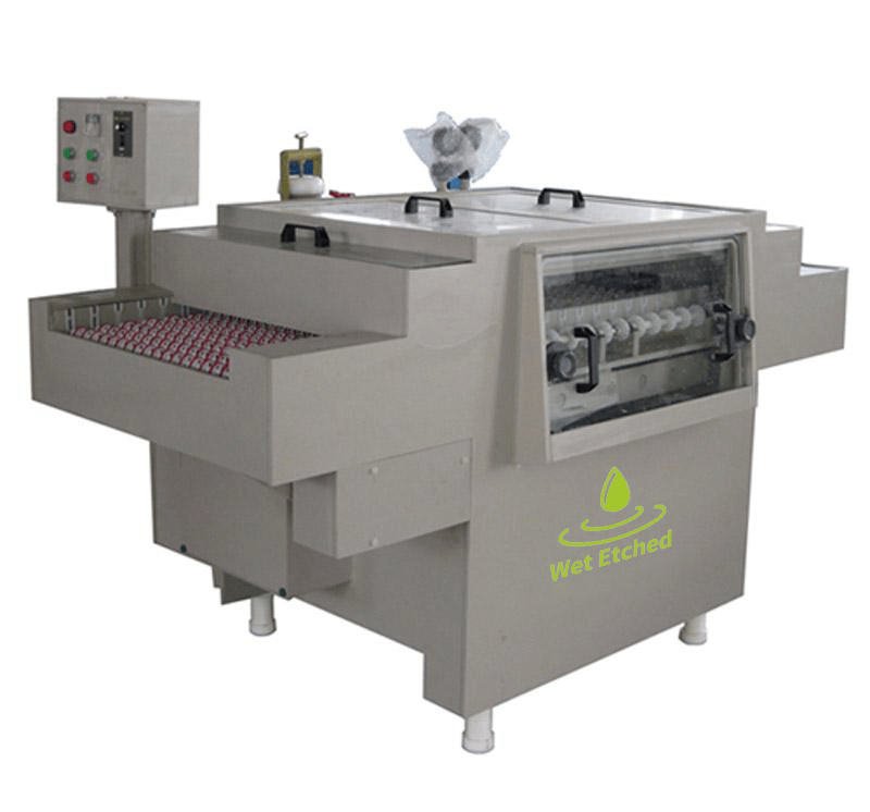
          Wet Chemical S650 Invar Etching Machine

          Wet Processing Equipment – Invar etching machine

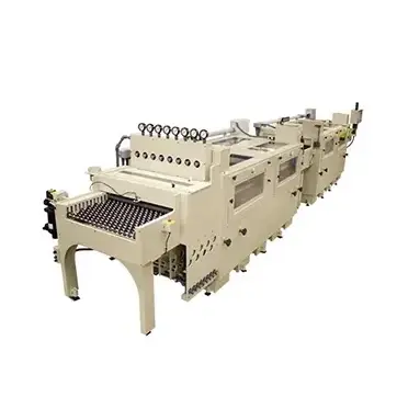
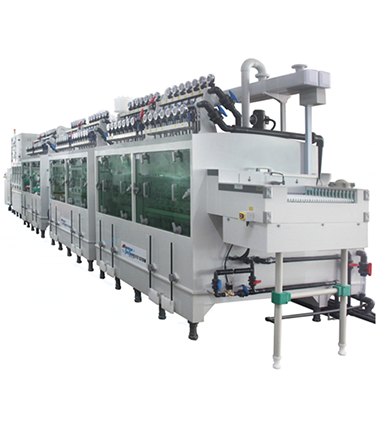
          The etching machine is used to spray chemical solution to a copper-clad laminator, aluminum substrate, or stainless steel plate, the exposed copper, aluminum, and stainless steel are etched away, retaining the pattern or circuit covered by the corrosion-proof film, so as to achieve the purpose of making pattern or circuit.

          This etching machine is an all-in-one small Invar etching machine that is easy to install and can be used immediately after powering on.

          Utilizing proper equipment is essential for achieving accurate and consistent results in the wet etching process. This includes:

          1. Chemical Tanks: Acid-resistant containers for holding the etching solution.
          2. Temperature Control Systems: Maintain a stable temperature during the etching process to ensure uniform results.
          3. Safety Equipment: Proper protective gear, such as gloves and goggles, should be worn to ensure safety during the handling of etchants.

          Photo Etching Invar:

          Photo etching is a precise process that allows for the creation of intricate designs on the surface of Invar. The process involves using a photoresist material to transfer a pattern onto the material, followed by selective etching.

          1. Photomasks: High-quality photomasks made of materials resistant to the etching solution are crucial for precise pattern transfer.
          2. UV Exposure Systems: Ensure controlled exposure to UV light during the photoresist process to achieve accurate and detailed patterns.

          View our metal etching products

          how to etch Invar?

          Invar Etching Process Guidelines:

          Below are general guidelines for wet etching Invar using common etchants:

          MetalEtchantTemperature (°C)Concentration (%)Estimated Etch Depth (microns)Etch Quality
          InvarNitric Acid (HNO3)Room temperature10-15% HNO31-10High-quality (smooth)
          InvarHCl and FeCl3 MixtureRoom temperatureVariable5-20Moderate-quality (etched)
          Invar Etching Process Guidelines

          Values provided are approximate and may vary based on specific etching conditions. Always conduct test etches and adjust parameters as needed for desired results. Safety precautions should be followed when handling chemicals.

          If you have metal wet etching Invar needs, please feel free to contact us.

            FAQs

            [FAQS]

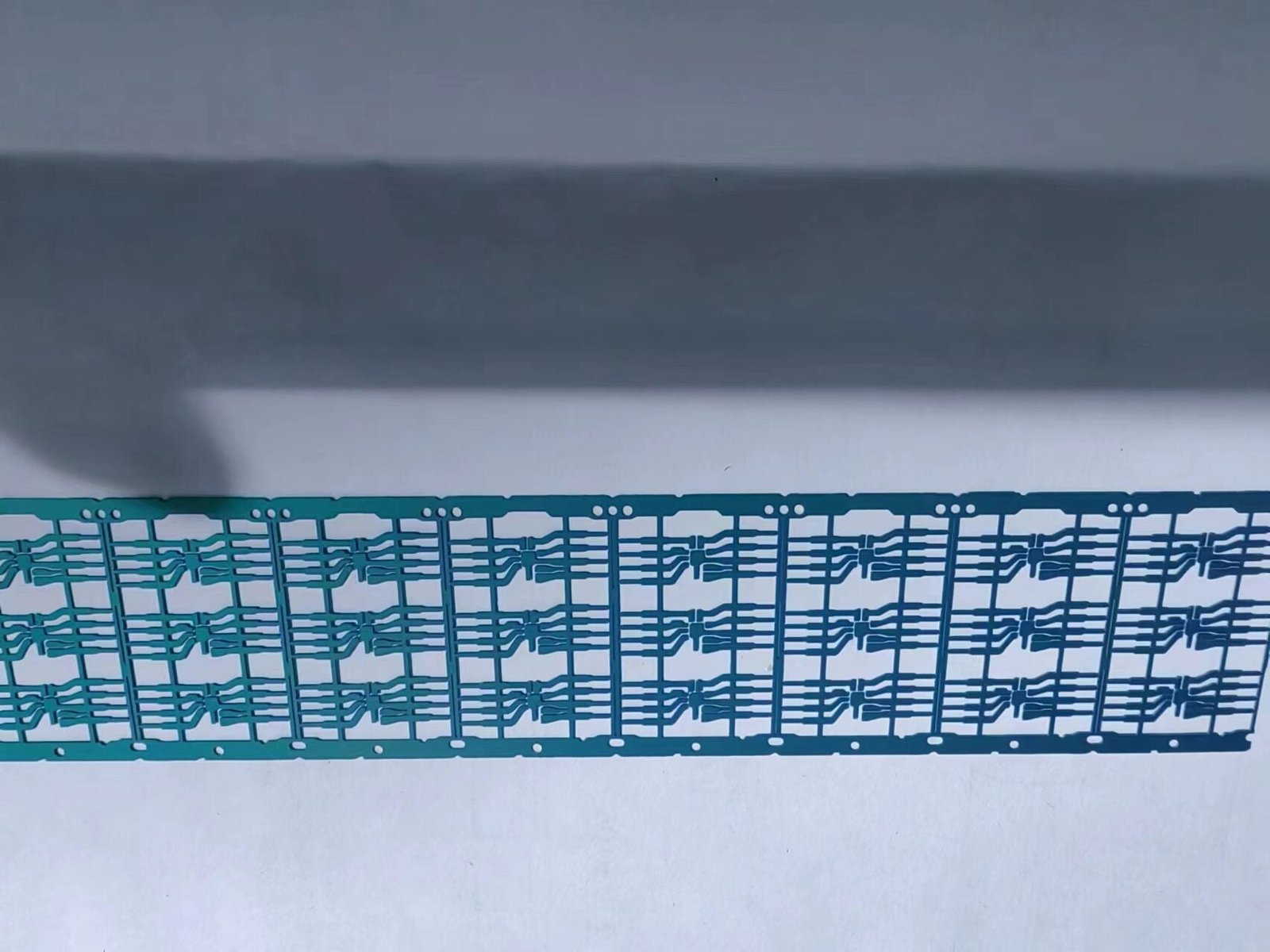
            Etching Invar Samples