Green Chemistry in Etching Solutions
As industries become more aware of their environmental footprint, the need for sustainable practices in manufacturing processes like chemical etching is growing. Green chemistry is at the forefront of these efforts, aiming to reduce the use of harmful chemicals and promote safer, more eco-friendly alternatives. In the realm of stainless steel etching, transitioning to less toxic acids and optimizing the etching process for environmental benefits is a crucial step toward sustainability.
Transition to Less Toxic Acids (Citric Acid Alternatives)
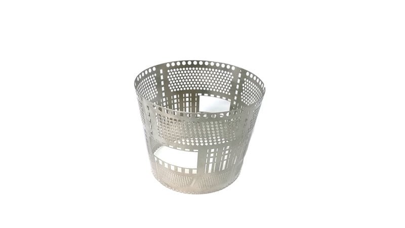
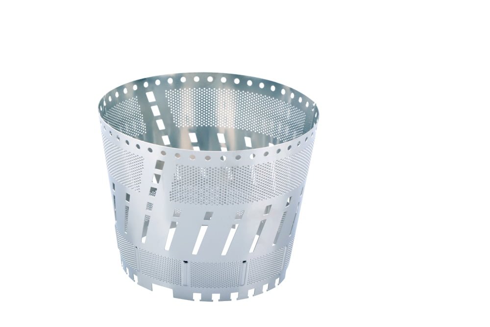
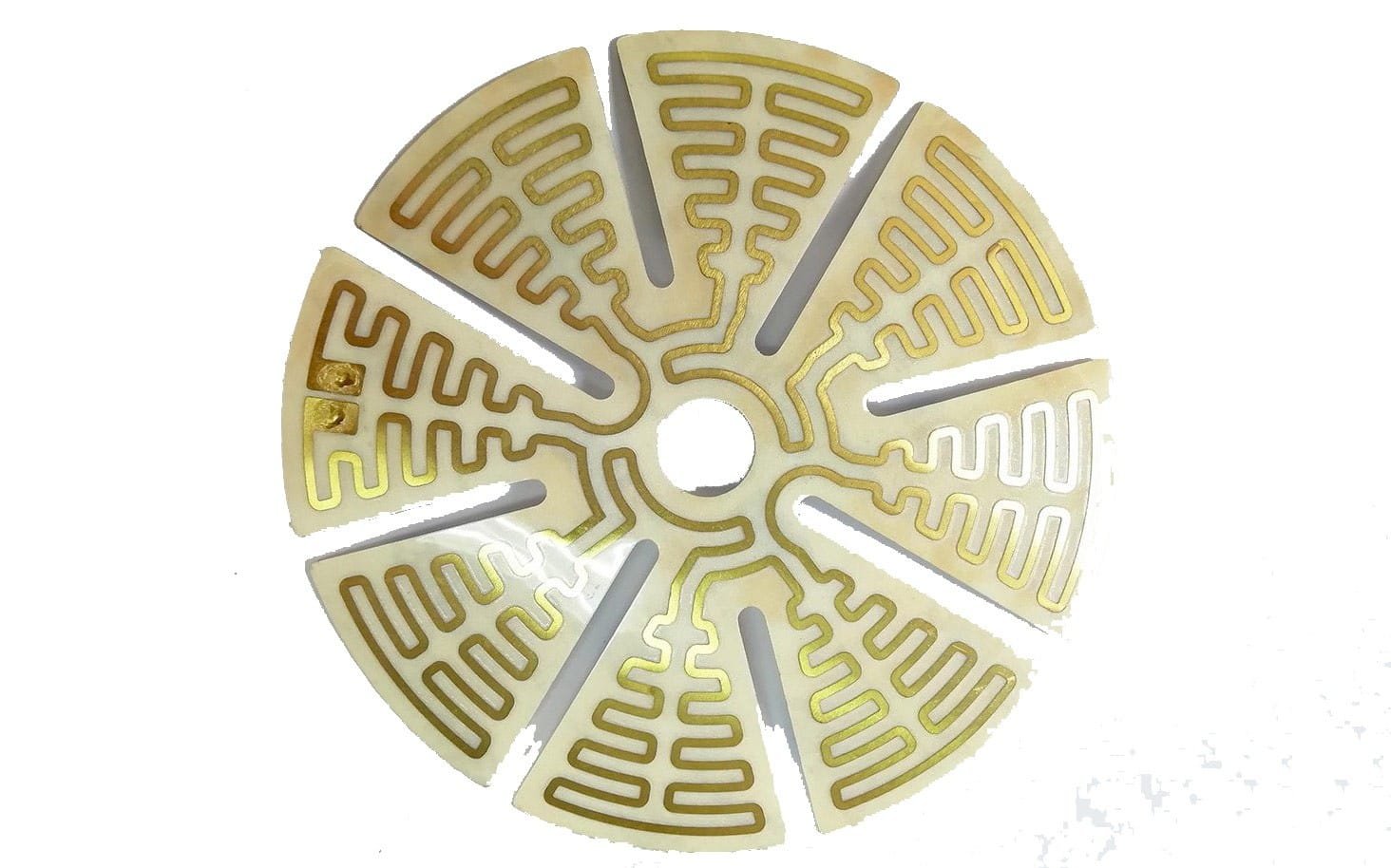
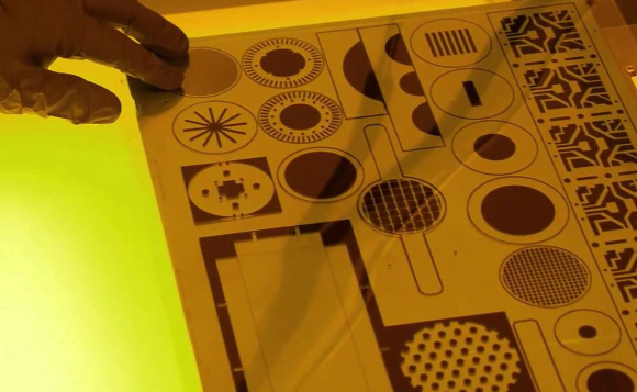
One of the most significant advancements in chemical etching has been the move away from toxic acids such as ferric chloride and nitric acid toward more eco-friendly alternatives. Citric acid, for example, has gained traction as a safer and more sustainable option for etching. It offers a similar etching power without the harmful environmental impact.
Benefits of Citric Acid-Based Solutions:
- Reduced toxicity: Less hazardous to both workers and the environment.
- Non-corrosive: Less damaging to equipment.
- Biodegradable: Does not persist in the environment, making disposal easier and safer.
By switching to citric acid and other safer alternatives, manufacturers can significantly lower their environmental risks and ensure a cleaner production process.
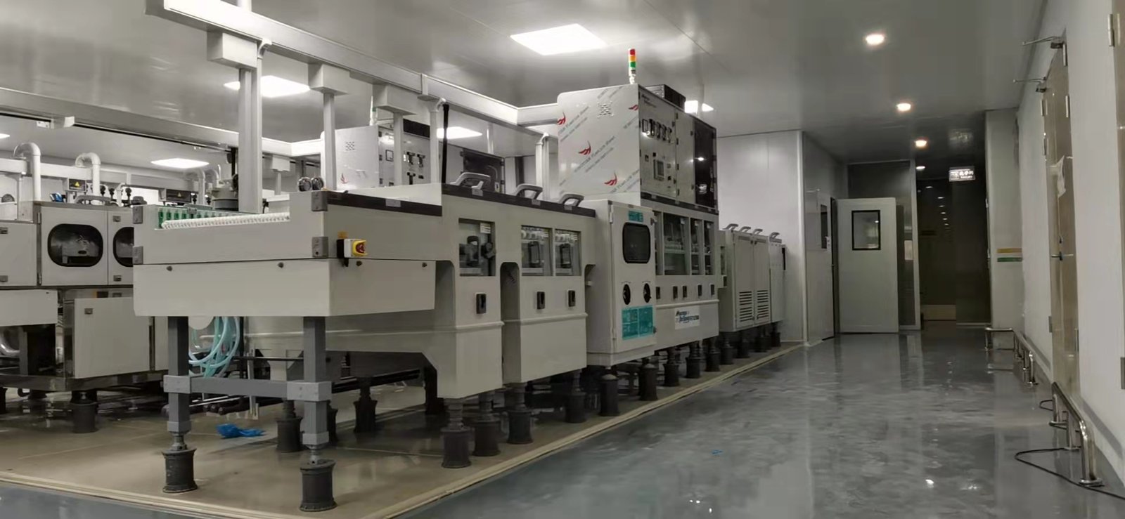
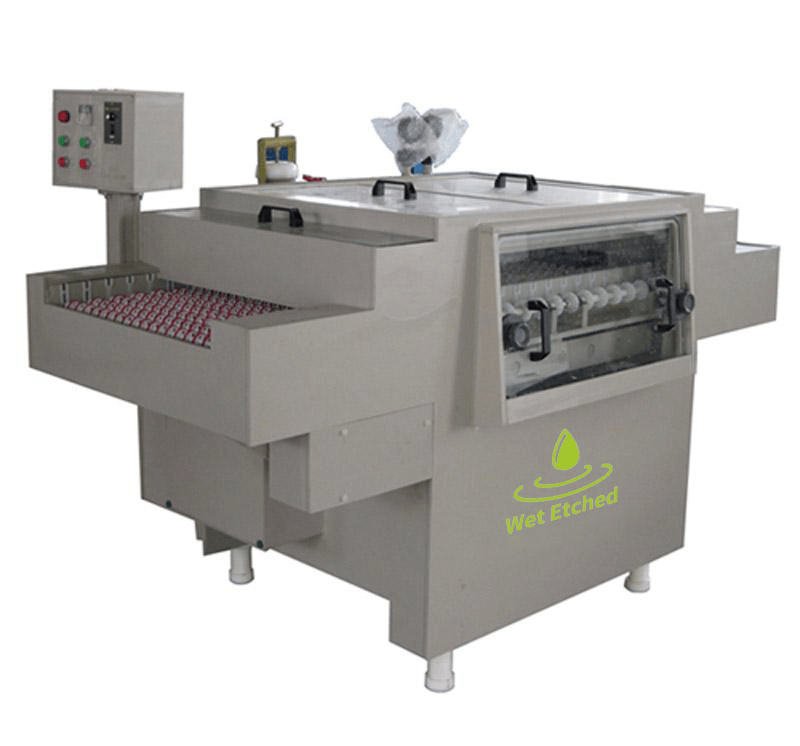
Closed-Loop Etching Systems
The closed-loop system in chemical etching is another vital aspect of sustainable production. These systems allow manufacturers to recapture and reuse etching chemicals, minimizing waste and reducing the need for fresh chemical supplies. With a closed-loop system, the etchant is filtered, neutralized, and purified, making it reusable for subsequent batches.
| Benefit | Traditional Etching | Closed-Loop System |
|---|---|---|
| Chemical Waste | High (frequent disposal required) | Low (chemicals are recycled) |
| Cost Efficiency | Higher due to chemical replenishment | Lower due to chemical reuse |
| Environmental Impact | High (disposal of toxic chemicals) | Minimal (reduces toxic waste) |
Implementing closed-loop systems is a cost-effective and environmentally friendly method for manufacturers looking to reduce their chemical waste and improve the sustainability of their production lines.
Waste Management and Recycling
Effective waste management is essential in reducing the environmental impact of chemical etching. Not only does this involve the careful disposal of harmful chemicals, but it also includes the recycling of metal scraps and other materials.
Neutralizing and Reusing Spent Etchants
A critical step in waste management is the neutralization of spent etchants. Once the etching solution has been used, it must be properly treated to neutralize harmful chemicals before disposal or reuse. By investing in neutralization systems, manufacturers can safely reuse spent etchants, thereby reducing waste and extending the life of the chemicals used in the process.
Scrap Metal Recycling Programs
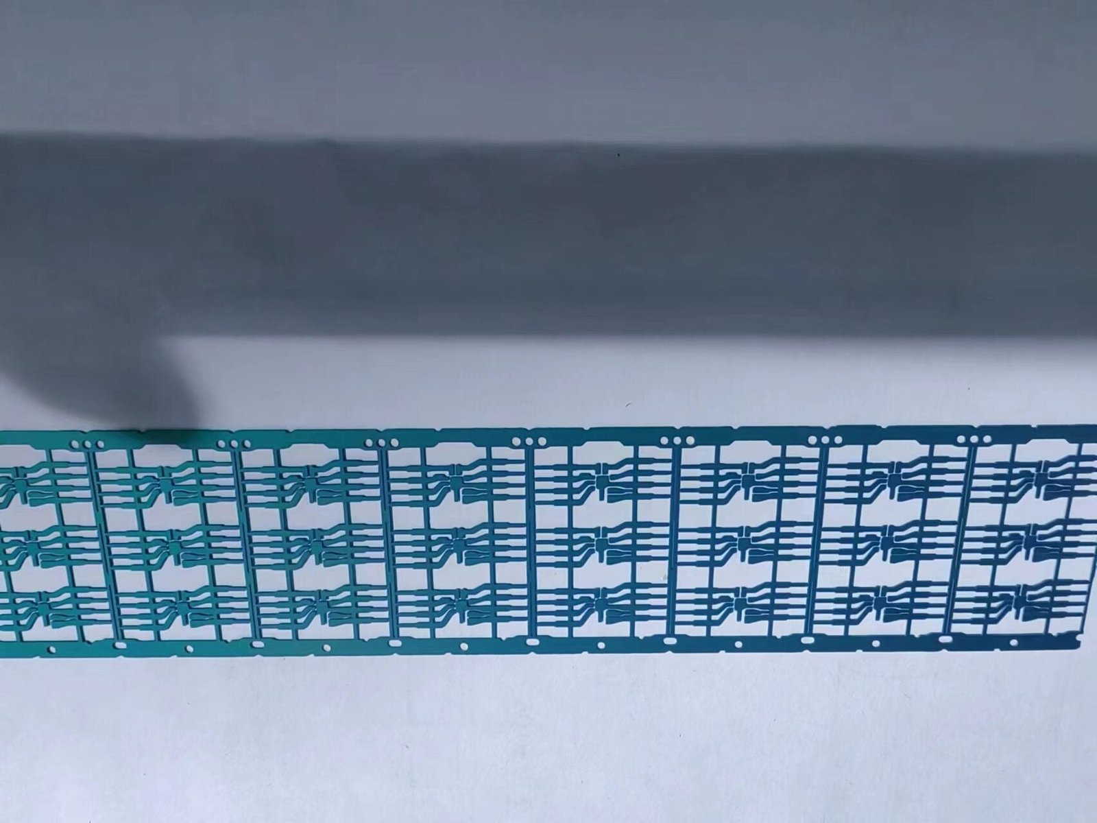
One of the most sustainable practices in chemical etching is the recycling of scrap metal. The stainless steel waste produced during the etching process can be collected, processed, and reused, reducing the need for virgin materials. This practice not only conserves resources but also decreases the carbon footprint associated with material sourcing.
Energy Efficiency in Production
Energy consumption is a significant factor in the sustainability of any manufacturing process. In chemical etching, optimizing energy usage can have a substantial positive effect on reducing the overall environmental impact of production.
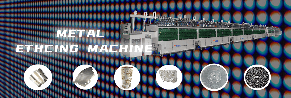
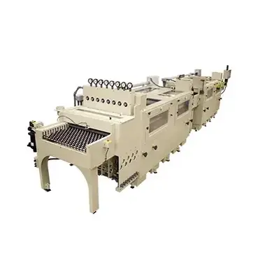
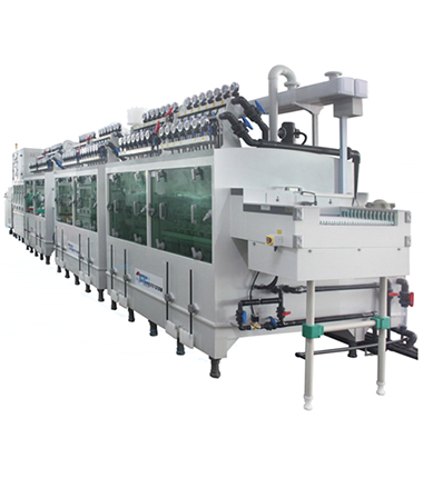
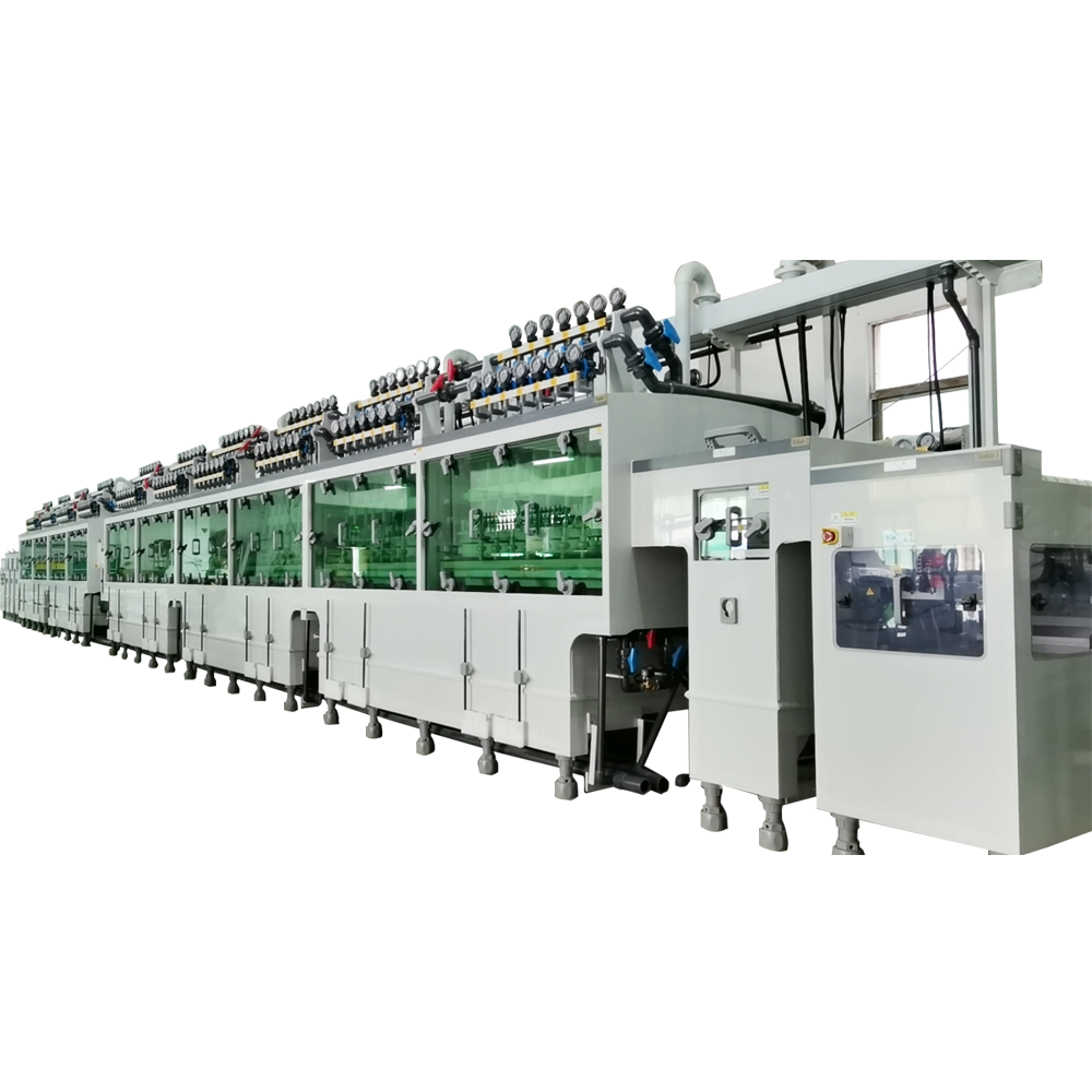
Low-Energy Etching Machines
Innovations in low-energy etching machines have made it possible for manufacturers to significantly cut energy consumption without sacrificing the quality of the etched product. These machines use advanced technology to minimize power usage while still providing the precision needed for high-quality etching.
Solar-Powered Facilities
To further reduce their carbon footprint, some manufacturers are turning to solar power for their production facilities. By investing in solar energy systems, companies can power their chemical etching operations using renewable energy, which drastically reduces reliance on fossil fuels and lowers CO2 emissions.
Certifications and Compliance
To stay ahead of evolving environmental regulations and meet the growing demand for sustainability, it is crucial for manufacturers to adhere to international standards and obtain relevant certifications.
ISO 14001 and REACH Compliance
Compliance with standards like ISO 14001 for Environmental Management and REACH (Registration, Evaluation, Authorization, and Restriction of Chemicals) is essential for manufacturers looking to demonstrate their commitment to environmental responsibility.
- ISO 14001 ensures that manufacturers are actively working to minimize their environmental impact and improve their sustainability practices.
- REACH compliance ensures that companies only use chemicals that are safe for human health and the environment.
These certifications help build trust with eco-conscious consumers and align the company with global sustainability initiatives.
Conflict-Free Material Sourcing
In addition to ensuring eco-friendly production practices, manufacturers must also focus on sourcing conflict-free materials. Ethical material sourcing, particularly in the case of metals, ensures that materials are procured in a way that does not contribute to environmental destruction or human rights violations.
Case Study: Zero-Waste Etching Facilities
Leading manufacturers in sustainable chemical etching are increasingly moving toward zero-waste facilities. These facilities focus on minimizing waste generation through closed-loop systems, recycling, and reducing overall material use.
How Leading Suppliers Achieve 95% Material Utilization
One leading supplier in zero-waste etching facilities has achieved 95% material utilization by effectively recycling scrap metal and reusing etchants. This significantly reduces the need for virgin materials and minimizes waste, making the production process more efficient and eco-friendly.
Carbon-Neutral Production Models
Another important step towards sustainability is adopting carbon-neutral production models. Some companies have already achieved carbon neutrality by offsetting their carbon emissions through the purchase of carbon credits or investing in renewable energy sources. These models contribute to overall environmental responsibility and set an example for other manufacturers to follow.