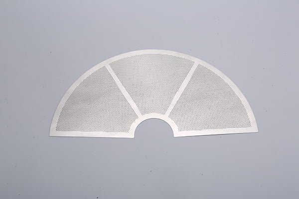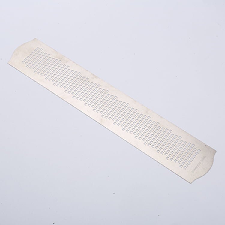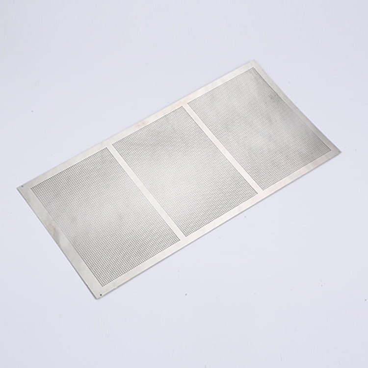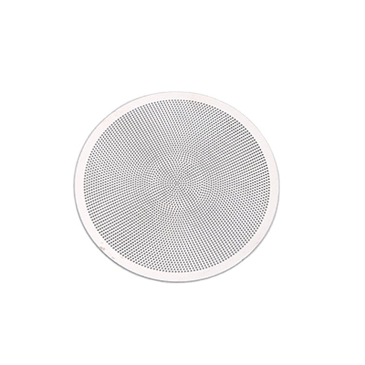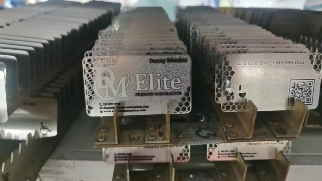
Photo Chemical Machining represents a cutting-edge approach in the fabrication of stainless steel components, offering unparalleled precision and flexibility. By understanding the electrochemical processes, mastering etchant selection, and employing advanced troubleshooting techniques, technical experts can push the boundaries of what’s possible in stainless steel manufacturing.

Electrochemical Principles of PCM for Stainless Steel
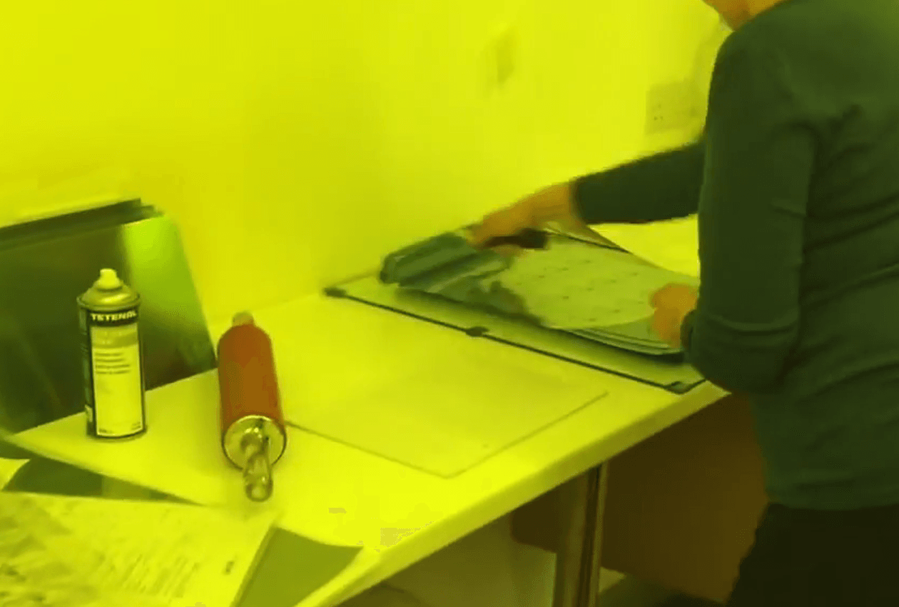
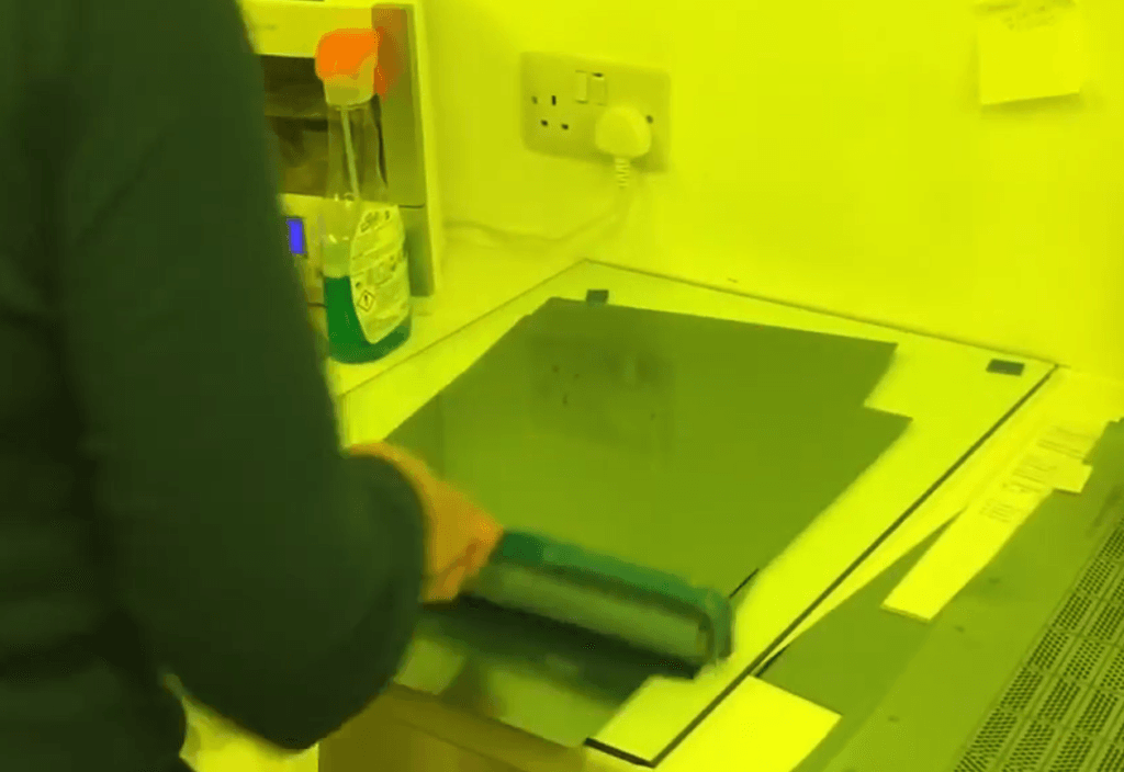
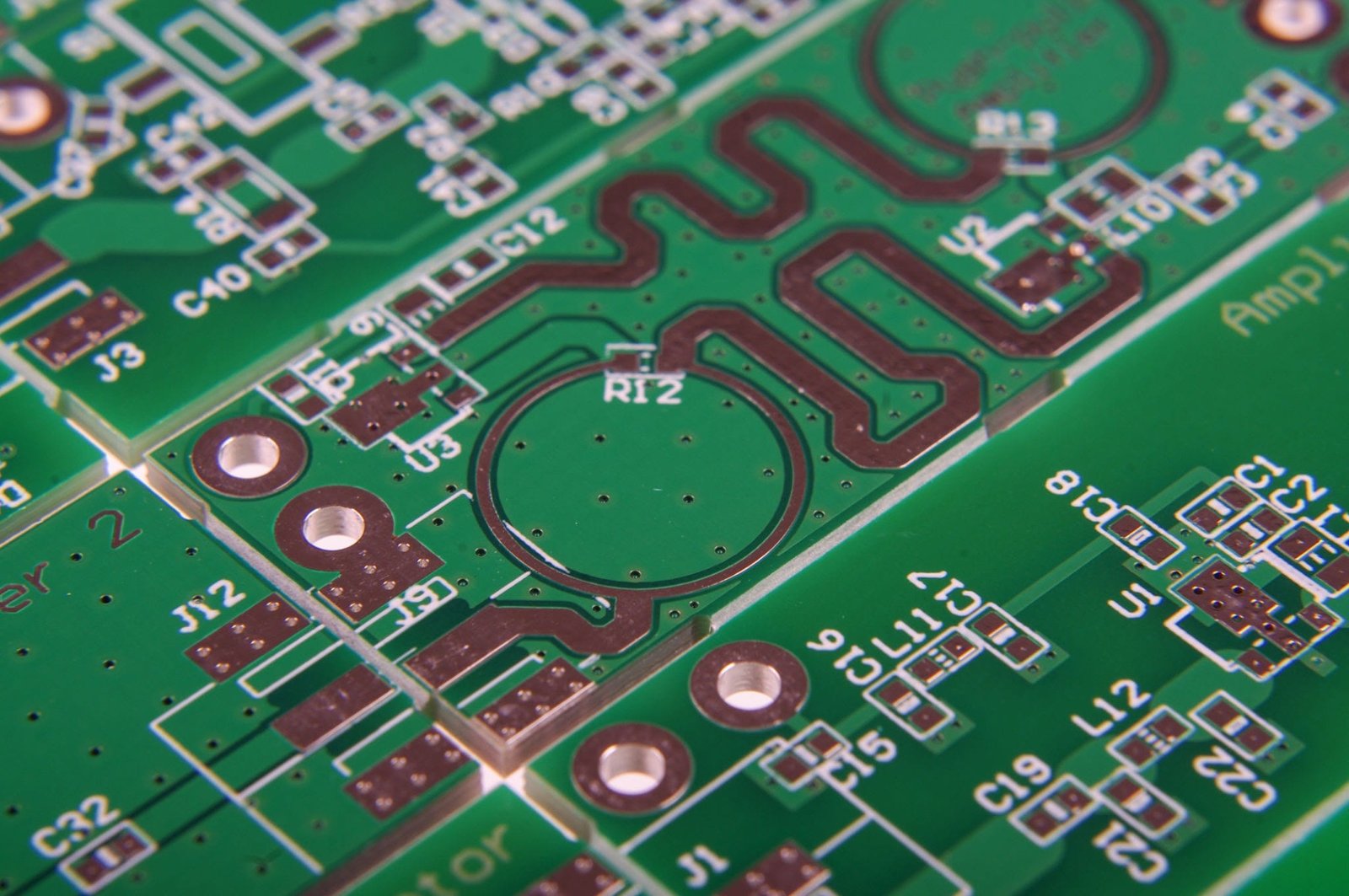
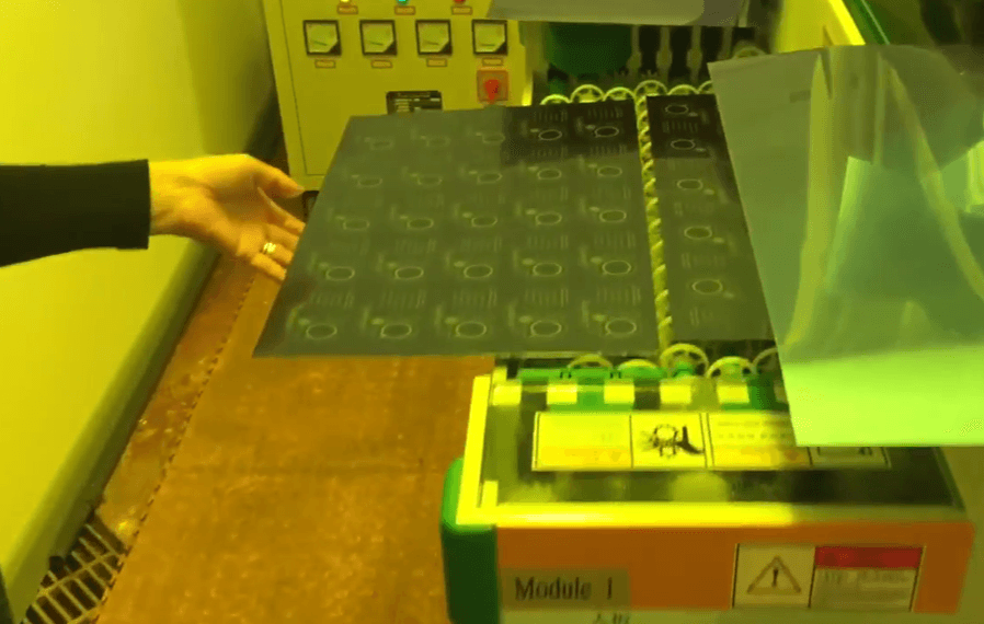
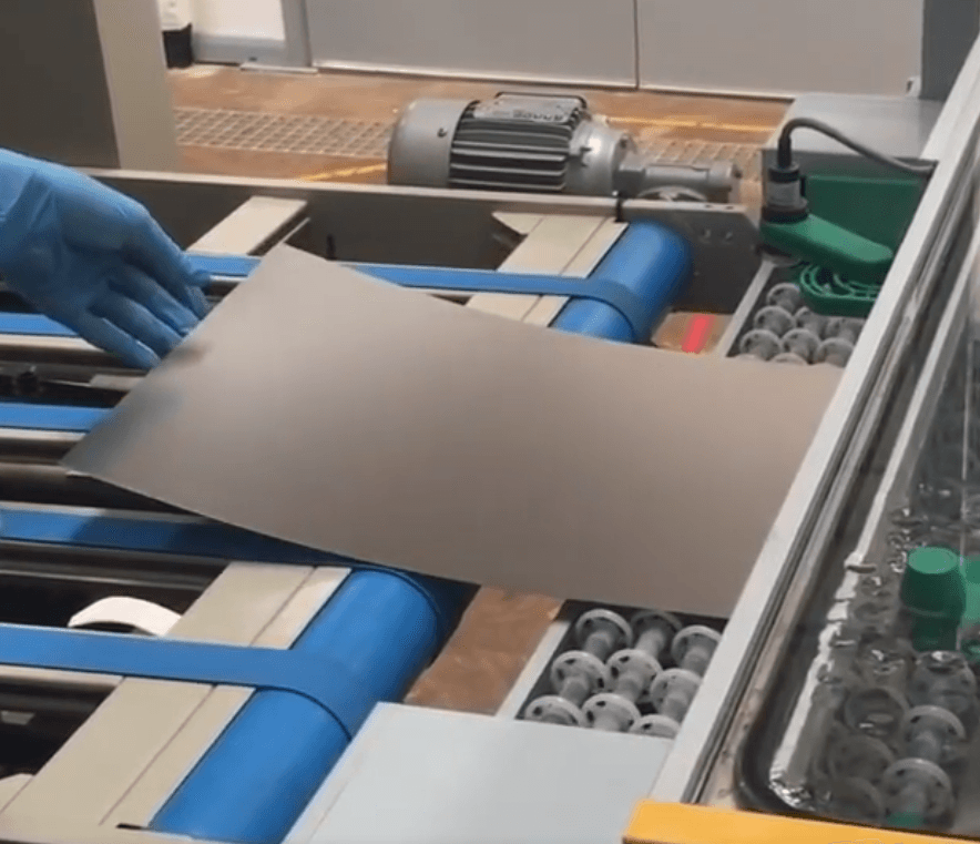
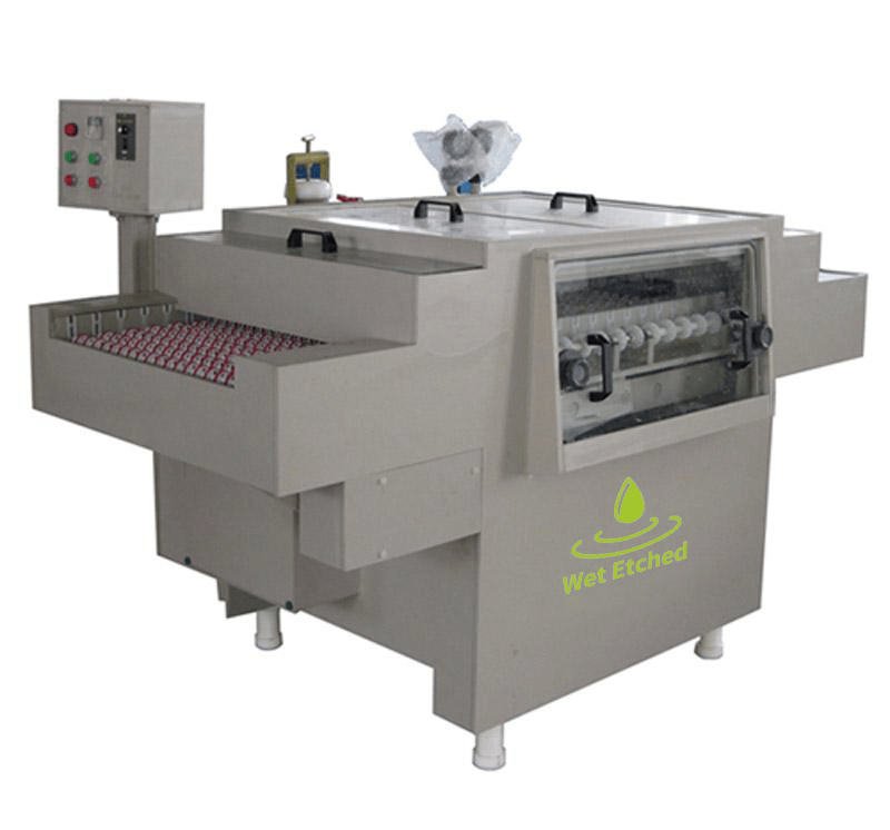
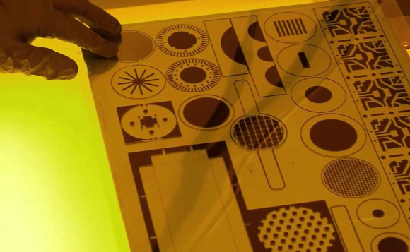
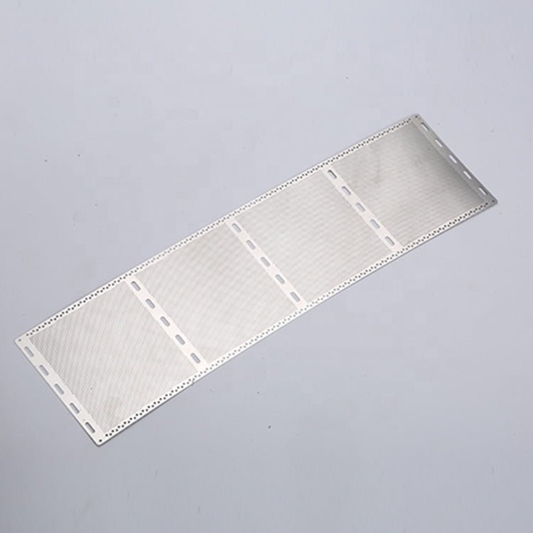
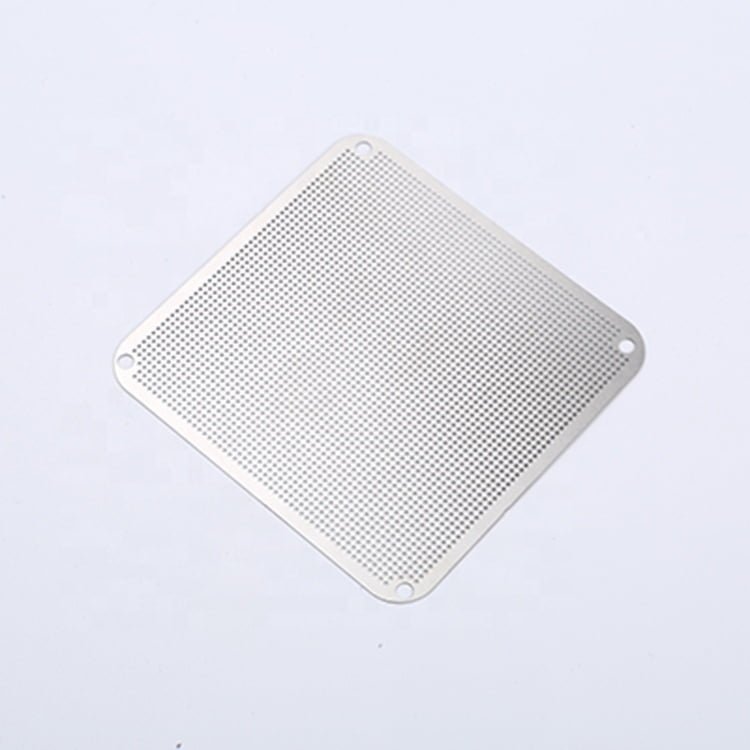
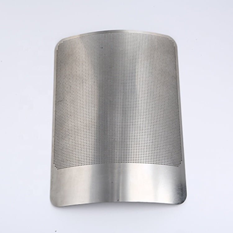
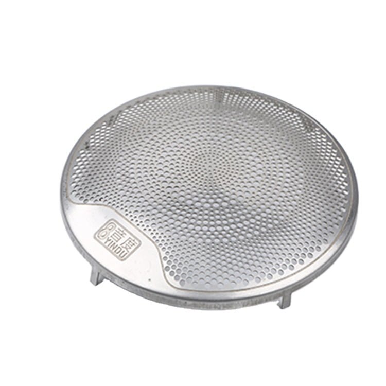
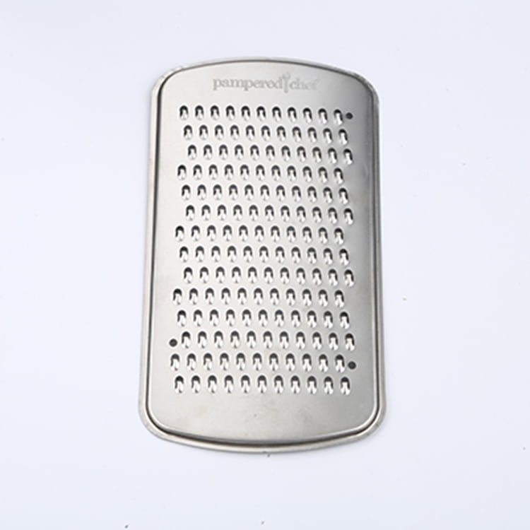
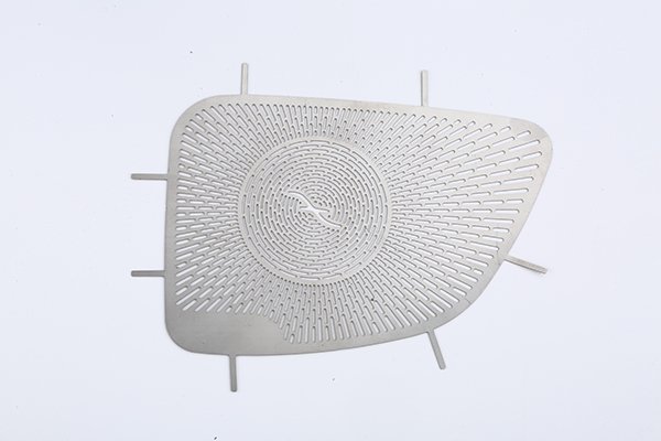
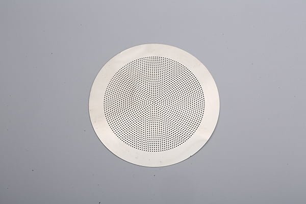
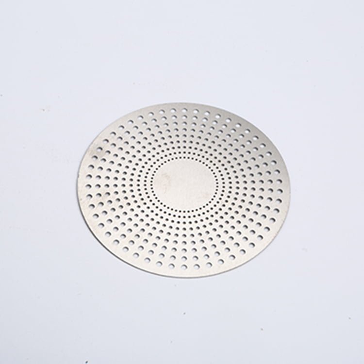
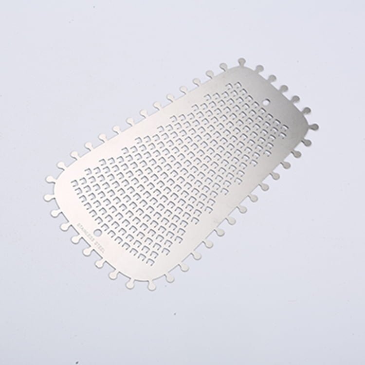
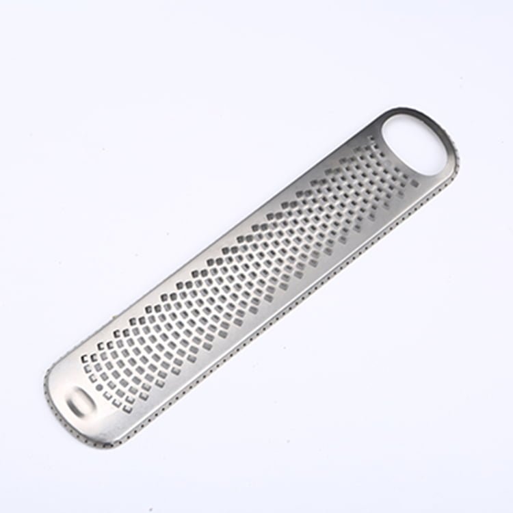
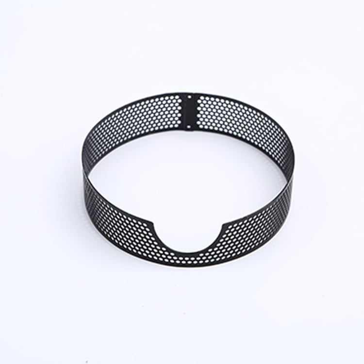
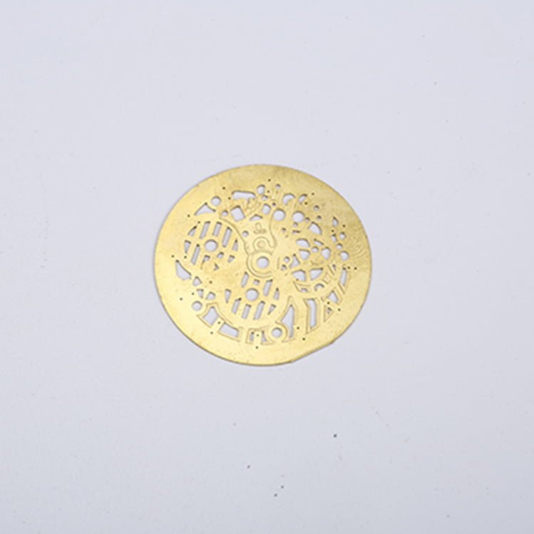
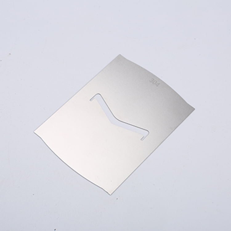
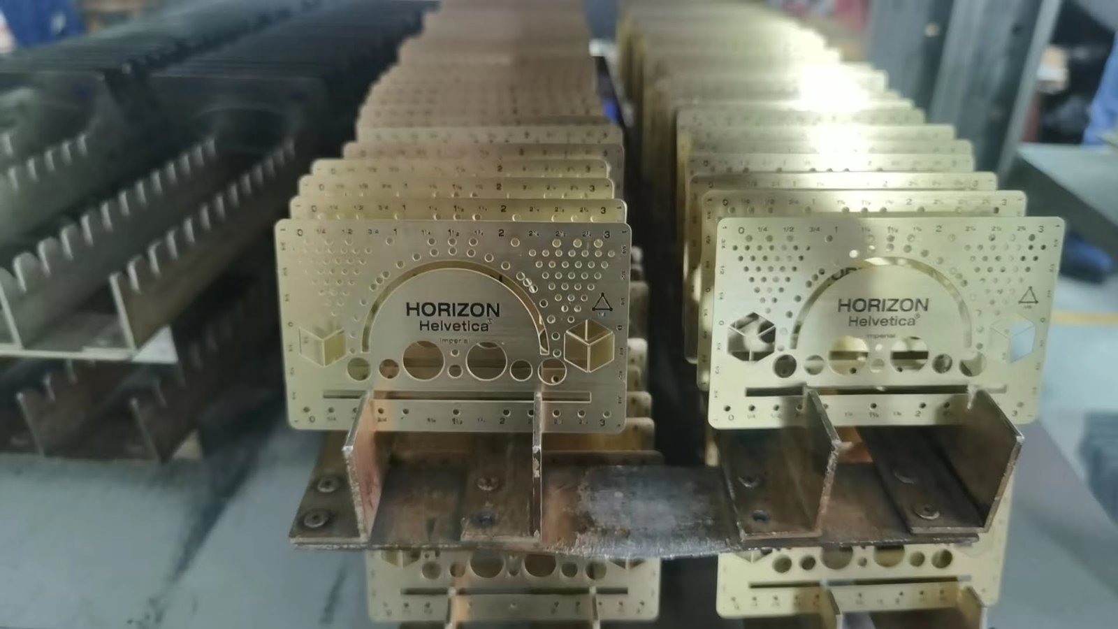
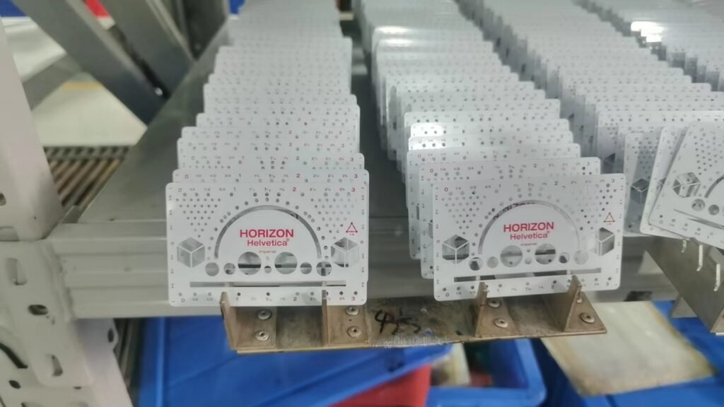
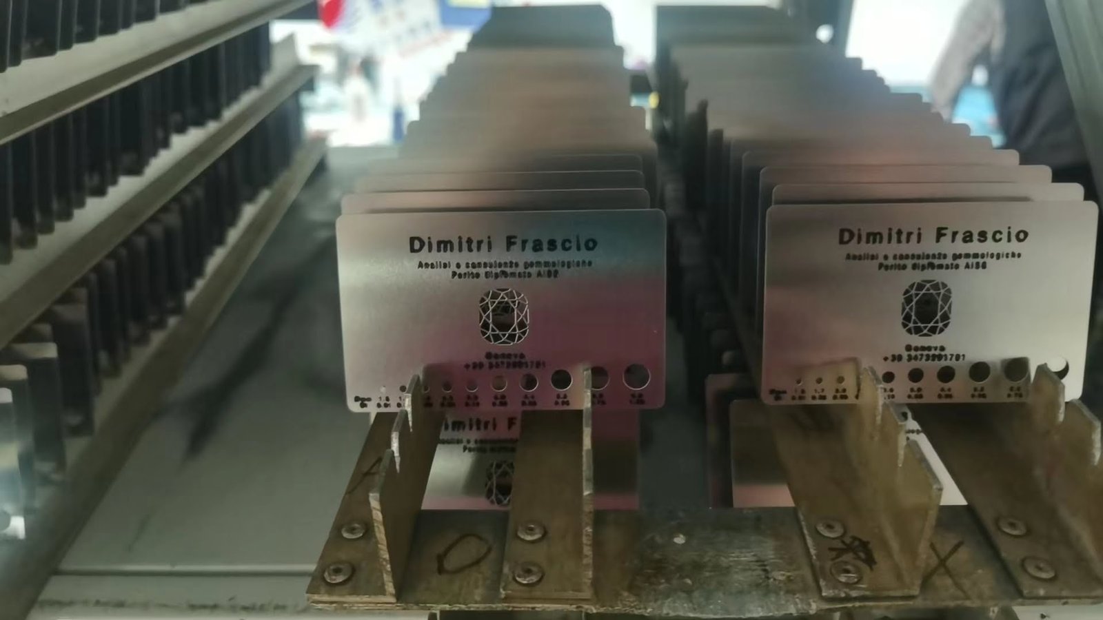
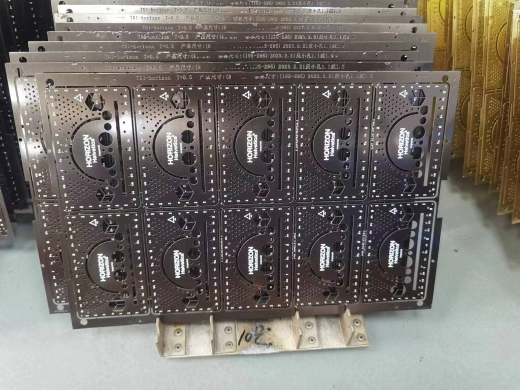
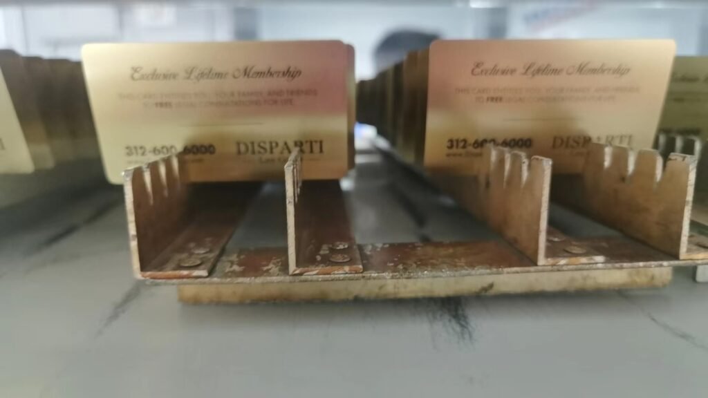
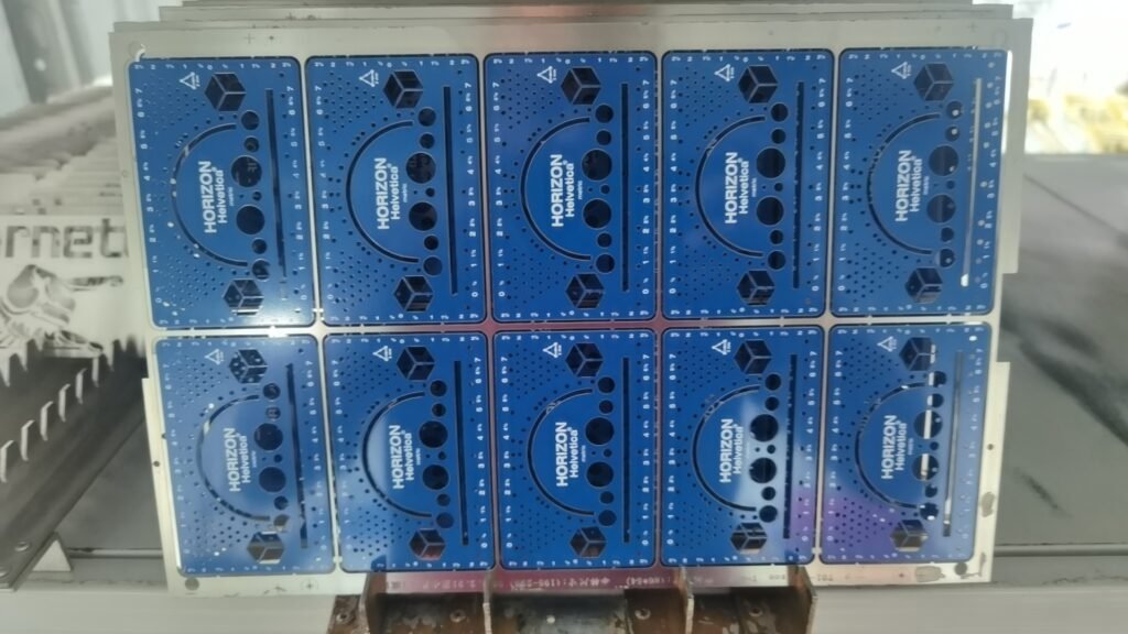
At its core, PCM leverages controlled electrochemical reactions to precisely remove unwanted metal from stainless steel surfaces. This process involves the use of specialized maskants that protect designated areas, ensuring that only the exposed regions are etched away.
Key elements include:
- Maskant Selection: The maskant must be compatible with both the substrate and the chosen etchant, ensuring a tight bond under aggressive chemical conditions.
- Etchant Chemistry: Common agents such as ferric chloride and nitric acid are used, where each offers distinct benefits in terms of reaction rate and surface finish.
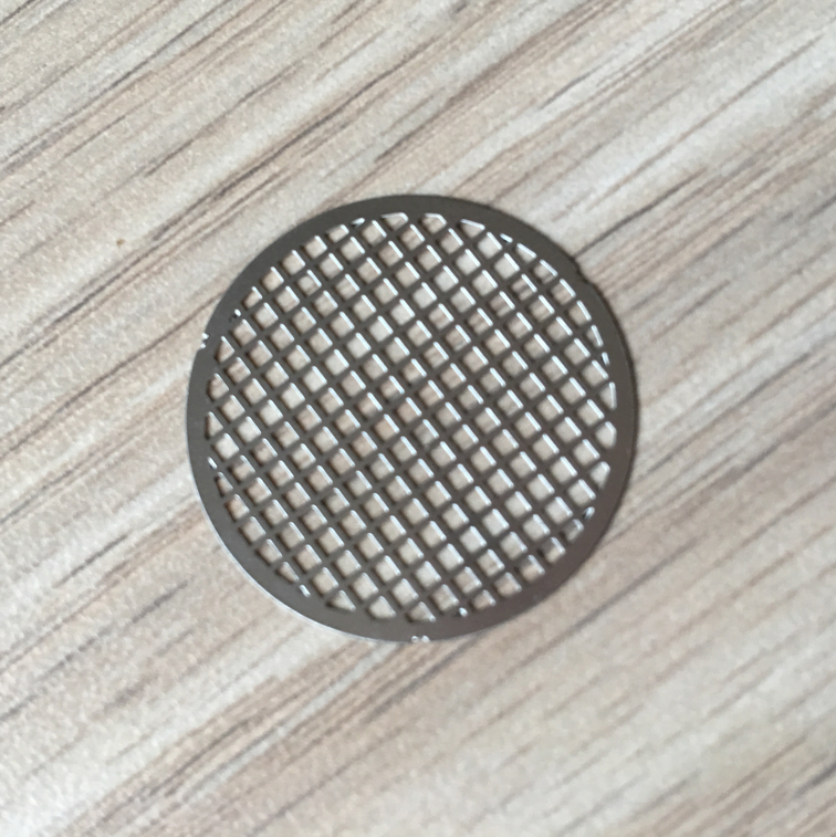
- Micron-Level Tolerance Control: Achieving micron-level precision demands rigorous monitoring of the etching time, temperature, and chemical concentration.
For additional insight on electrochemical machining techniques, industry experts at Automation World offer a wealth of resources on related manufacturing processes.
Case Study: Optimizing Etch Rates for 316L Stainless Steel in Medical Device Components
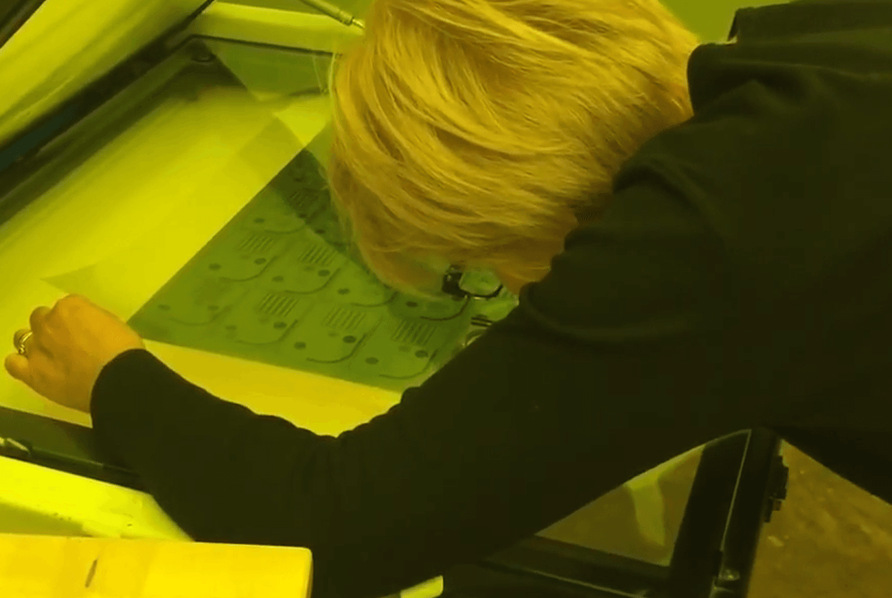
A prime example of PCM’s efficacy is its application in the fabrication of medical device components using 316L stainless steel. Manufacturers have optimized etch rates by carefully balancing etchant concentration and exposure times, resulting in components with exceptional tolerances required for medical applications.
This case study not only emphasizes the importance of process control but also illustrates how small adjustments in chemical formulation can significantly reduce common issues such as over-etching and undercut defects. Detailed analyses, including Scanning Electron Microscope (SEM) micrographs, have enabled engineers to fine-tune process parameters and enhance yield.
Leading industry voices, such as those featured on Advanced Manufacturing, underline the transformative potential of PCM in ensuring high-quality, reliable components in the medical field.
Troubleshooting Common Defects with SEM Micrograph Analysis
Despite its precision, PCM is not without challenges. Undercut and over-etching are common defects encountered during the process.
Troubleshooting strategies include:
- SEM Analysis: Utilizing SEM micrograph analysis can help identify the onset of undercutting, allowing for early interventions.
- Process Optimization: Adjusting the concentration of etchants and modulating temperature profiles are effective methods to mitigate defects.
- Regular Calibration: Continuous monitoring and calibration of equipment ensure that the process remains within set parameters, thereby reducing defect rates.
By integrating regular SEM inspections into the workflow, fabricators can maintain consistent quality and enhance the overall reliability of PCM processes.
Comparison Table: PCM vs. Laser Cutting for Thin-Gauge Stainless Steel
When it comes to thin-gauge stainless steel (0.1–2.0 mm), choosing between PCM and laser cutting hinges on several critical factors. The table below summarizes the primary differences:
| Aspect | Photo Chemical Machining (PCM) | Laser Cutting |
|---|---|---|
| Precision | Micron-level tolerance control achievable | High, but can be less consistent for ultra-thin gauges |
| Heat-Affected Zone (HAZ) | No significant HAZ, ideal for sensitive applications | Often produces a noticeable HAZ |
| Material Stress | Minimal stress introduced to the workpiece | Can induce thermal stress, potentially affecting integrity |
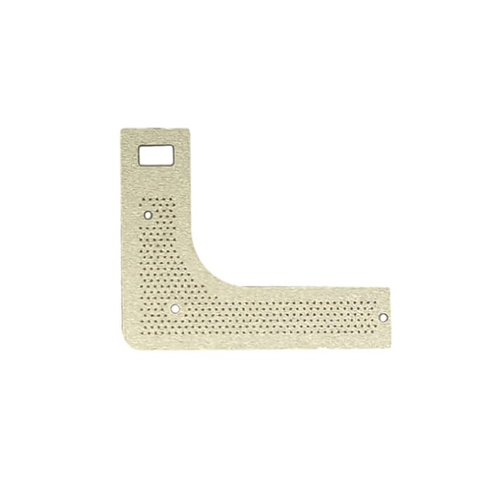
| Complex Geometry | Excellent for intricate designs due to the maskant technique | Well-suited, but may require additional finishing |
| Process Complexity | Requires strict chemical and process control procedures | More straightforward but less flexible for micro-details |
| Cost Efficiency | Often lower for high-volume, precision applications | Economical for rapid prototyping and large panels |
Table: Detailed comparison highlighting the strengths and limitations of PCM versus laser cutting for thin-gauge stainless steel.
This comparative analysis allows manufacturers to select the appropriate cutting method based on their specific application requirements and quality control demands.
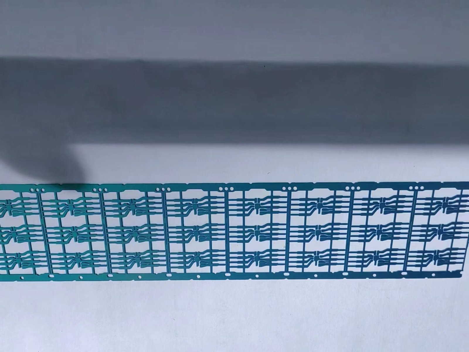
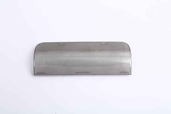
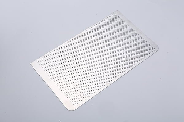
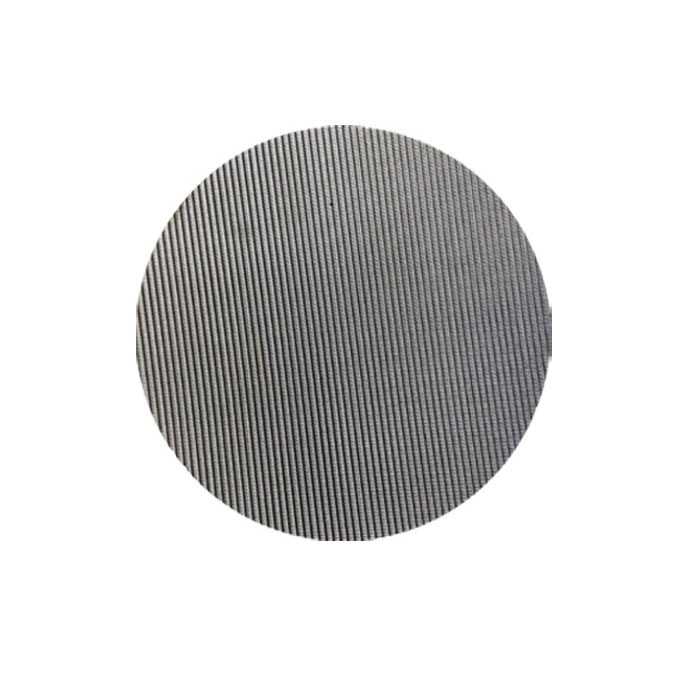
Advanced Techniques: Hybrid Processes for EMI Shielding Grids
In recent years, hybrid processes that combine PCM with micro-stamping have emerged, particularly for the production of EMI shielding grids. This integrated approach leverages the chemical precision of PCM with the forming efficiency of micro-stamping, delivering parts with superior performance characteristics.
Key advantages of these hybrid techniques include:
- Enhanced Material Properties: By combining processes, fabricators can produce parts with improved electrical and mechanical performance.
- Optimized Production Rates: Hybrid processes reduce cycle times while maintaining high quality, contributing to overall cost savings.
- Customizable Solutions: Tailored process parameters allow for the production of components that meet the unique demands of different electronic applications.
For further case studies and insights into advanced hybrid manufacturing methods, Industry Today provides comprehensive resources and expert commentary.