The next wave of thin film heating technology is marked by innovation and integration with cutting-edge solutions like smart sensors, graphene-enhanced films, and AI. These advancements are paving the way for more efficient, sustainable, and intelligent heating solutions across industries, from wearable tech to space exploration. As the demand for smarter, more energy-efficient solutions grows, thin film heaters will continue to play a crucial role in shaping the future of heating technology.
Smart Heaters: Embedded Sensors and IoT Connectivity
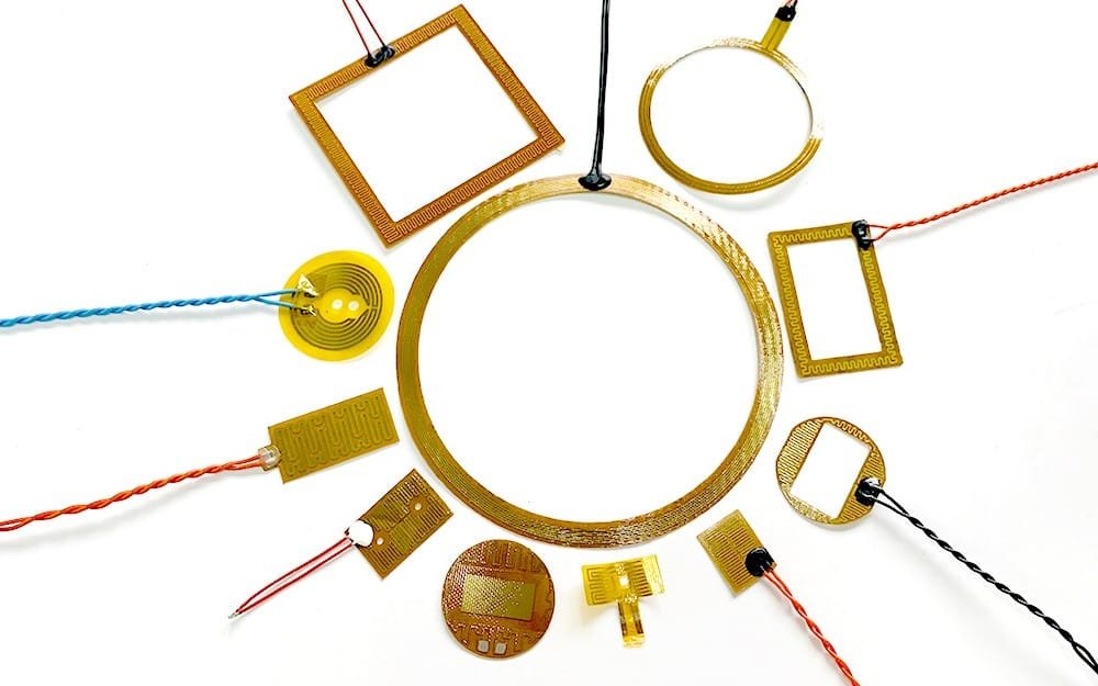
The integration of smart sensors and IoT connectivity is transforming the world of thin film heating technology, making it possible to create heating solutions that are not only efficient but also responsive to changing conditions.

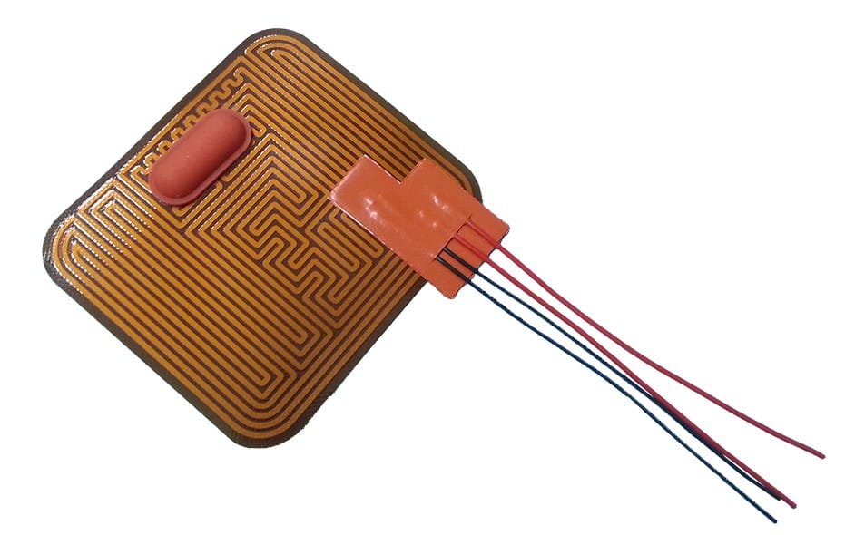
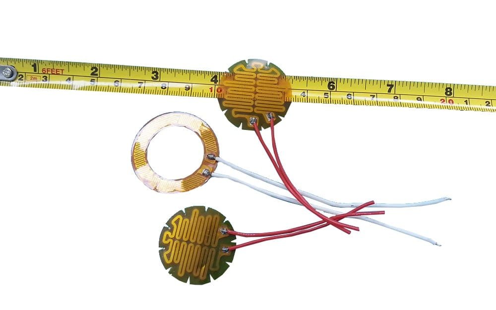
- Embedded Sensors: Smart heaters equipped with temperature sensors offer real-time feedback to ensure precise temperature regulation. For instance, in medical devices such as IV tube warmers or CPAP machines, these sensors help maintain a stable temperature, improving patient safety and comfort. By continuously monitoring the temperature, these systems can automatically adjust heating output to prevent overheating or underheating, offering a higher level of control than traditional systems.
- IoT Connectivity: The rise of Internet of Things (IoT) connectivity further enhances the functionality of thin film heaters. IoT-enabled heaters can communicate with other devices, allowing for remote monitoring and control. This is especially beneficial in electric vehicle (EV) battery management systems, where thin film heaters embedded in battery packs can be remotely monitored to ensure that the batteries are always operating within the optimal temperature range. These systems can send real-time alerts to the user or maintenance team if the temperature strays from the desired range, enabling proactive adjustments and reducing the risk of thermal issues.
The combination of smart sensors and IoT connectivity is ushering in a new era of intelligent heating solutions, offering not only improved efficiency but also enhanced safety and reliability.
Energy Efficiency Breakthroughs
Energy efficiency is a key consideration in the development of future heating technologies. With growing concerns over sustainability, the next generation of thin film heaters will be focused on reducing energy consumption while still delivering high-performance results.
- Graphene-Enhanced Films: One exciting development in the world of thin film heaters is the incorporation of graphene—a material known for its exceptional electrical conductivity and thermal properties. Graphene-enhanced heating films can offer faster heat-up times and more even heat distribution, while using less energy. These films can be used in a variety of applications, including wearable tech and smart homes, providing sustainable heating without sacrificing performance.
- Low-Voltage Designs: Another key trend in energy efficiency is the development of low-voltage heating solutions. Low-voltage thin film heaters are particularly well-suited for portable and wearable applications, where reducing power consumption is critical. These heaters can operate on a lower voltage (5V to 12V), making them safer and more energy-efficient for personal devices, such as heated clothing, smart gloves, and battery-powered heating pads. As demand for energy-efficient solutions grows, these low-voltage designs will become more common in consumer products and electronic devices.
The future of thin film heaters is leaning heavily toward energy-efficient breakthroughs, with technologies like graphene and low-voltage designs paving the way for sustainable and cost-effective heating solutions.
Wearable Tech: Heating in Clothing and Health Monitors
The wearable tech market is expanding rapidly, and thin film heaters are at the forefront of this revolution. These heaters offer the perfect combination of flexibility, lightweight design, and energy efficiency, making them ideal for incorporation into smart clothing and health monitoring devices.

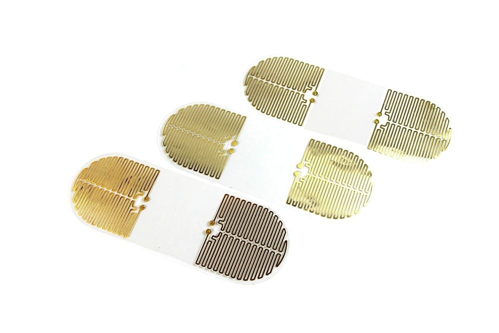
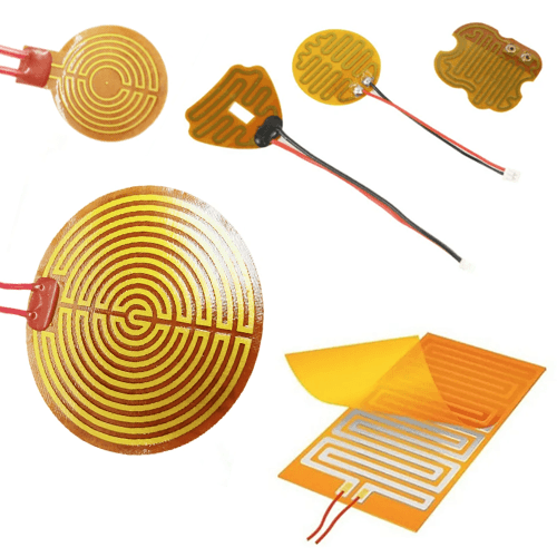
- Ultrathin, Skin-Safe PET Heaters: PET-based thin film heaters are particularly popular in wearable applications due to their ultrathin design and skin-safe properties. These heaters can be seamlessly integrated into therapeutic wearables, such as heating patches for pain relief or smart clothing that keeps the wearer warm in cold environments. The flexibility of PET allows the heater to conform to the body, providing uniform heat distribution without adding bulk or discomfort.
- Health Monitoring Devices: In addition to providing warmth, thin film heaters are also finding use in health monitors that track the wearer’s body temperature or provide therapeutic heat to sore muscles. These devices are designed to be lightweight and portable, providing an added layer of functionality for athletes, elderly individuals, or anyone in need of personalized thermal therapy.
As the wearable tech market continues to grow, the demand for thin, flexible, and energy-efficient heating elements will only increase. Thin film heaters provide a convenient and effective solution for manufacturers looking to create high-performance wearable devices.
Space and Aerospace Applications
The need for high-performance heating solutions is even more critical in space and aerospace applications, where materials must withstand extreme environmental conditions. PI-based thin film heaters have become an essential component in many space missions, including satellite components and Mars rover systems.
- Extreme Temperature Resilience: Polyimide (PI) is known for its ability to withstand extreme temperatures, making it ideal for use in outer space, where temperature fluctuations can range from extreme heat to extreme cold. PI-based heaters are used to regulate the temperature of critical components, such as satellite electronics or rover instruments, ensuring they remain operational in harsh conditions.
- Thermal Management in Spacecraft: In spacecraft, PI heaters help maintain the temperature of sensitive equipment, preventing freezing or overheating. The material’s flexibility and lightweight nature make it perfect for integration into space modules, where minimizing weight is crucial for launch and flight efficiency.
As space exploration progresses, the role of thin film heaters will continue to grow, offering critical thermal regulation in the most challenging environments.
The Road Ahead: Self-Regulating Heaters and AI Integration
Looking ahead, the future of thin film heating technology is set to be shaped by artificial intelligence (AI) and self-regulating systems that will further enhance heating performance and longevity.
- AI-Driven Adaptive Heating: AI integration is one of the most promising advancements in smart heating systems. By embedding machine learning algorithms into thin film heaters, these systems can adapt in real-time to changing conditions. For example, smart homes could use adaptive heating to adjust room temperatures based on occupancy or external weather conditions. The system would learn the user’s preferences and optimize heating for comfort and efficiency, reducing energy consumption and enhancing overall user experience.
- Self-Repairing Materials: Another exciting development is the integration of self-repairing materials into thin film heaters. These materials have the ability to automatically detect and repair any damage or wear over time, ensuring that the heater continues to perform at optimal levels. Self-repairing heaters could greatly extend the lifespan of heating elements in consumer electronics, automotive systems, and industrial applications.
The future of thin film heating technology is full of possibilities, with AI-driven adaptive systems and self-repairing materials poised to revolutionize the way we use and maintain heating devices.