Category Archives: Blog

Your blog category

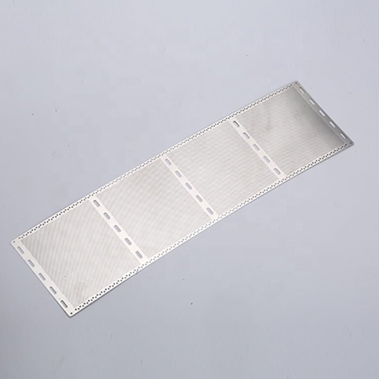
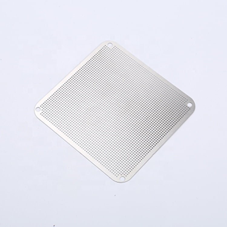
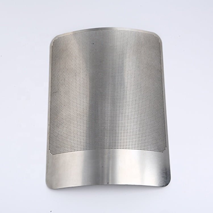
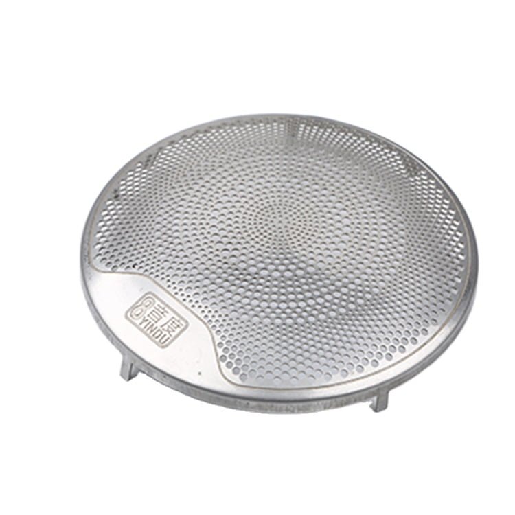
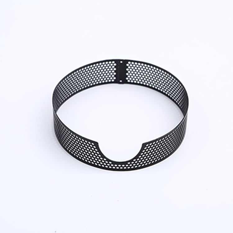
The Chemical Etching Molybdenum Process: Precision and Innovation with WET Etched

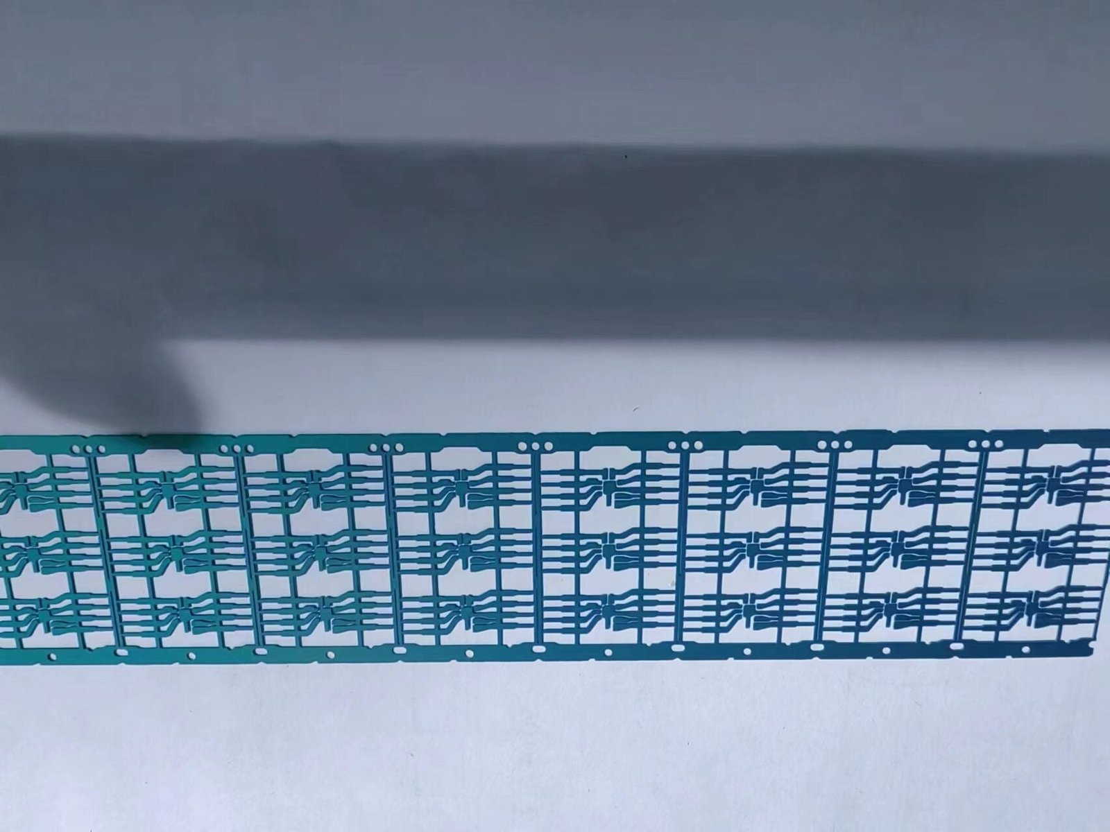
The chemical etching process for molybdenum creates precision components by selectively removing metal through a photoresist mask. This advanced technique offers numerous advantages over conventional sheet metalworking, including the ability to produce parts without degrading material properties, as no force or heat is used during processing. It also allows for almost limitless part complexity, with component features machined simultaneously using etchant chemistries.

What is Chemical Etching Molybdenum and How Does It Work?

Chemical etching molybdenum is a metalworking process that utilizes specialized corrosive chemicals to etch complex and precise components from molybdenum. This process is highly favored in modern metal machining due to its high precision, low failure rate, and the unique properties of molybdenum, such as its high melting point and excellent strength at elevated temperatures.

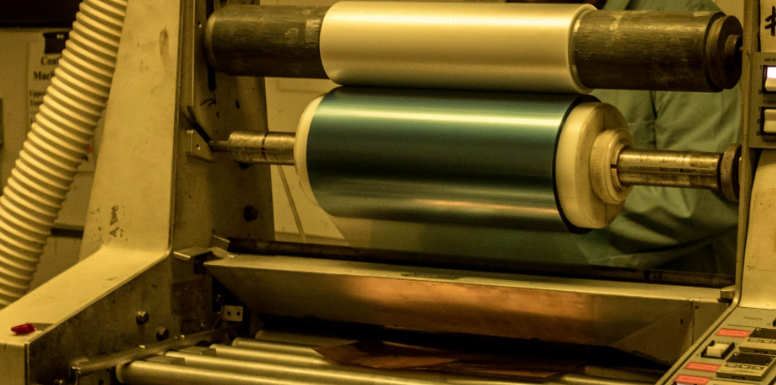
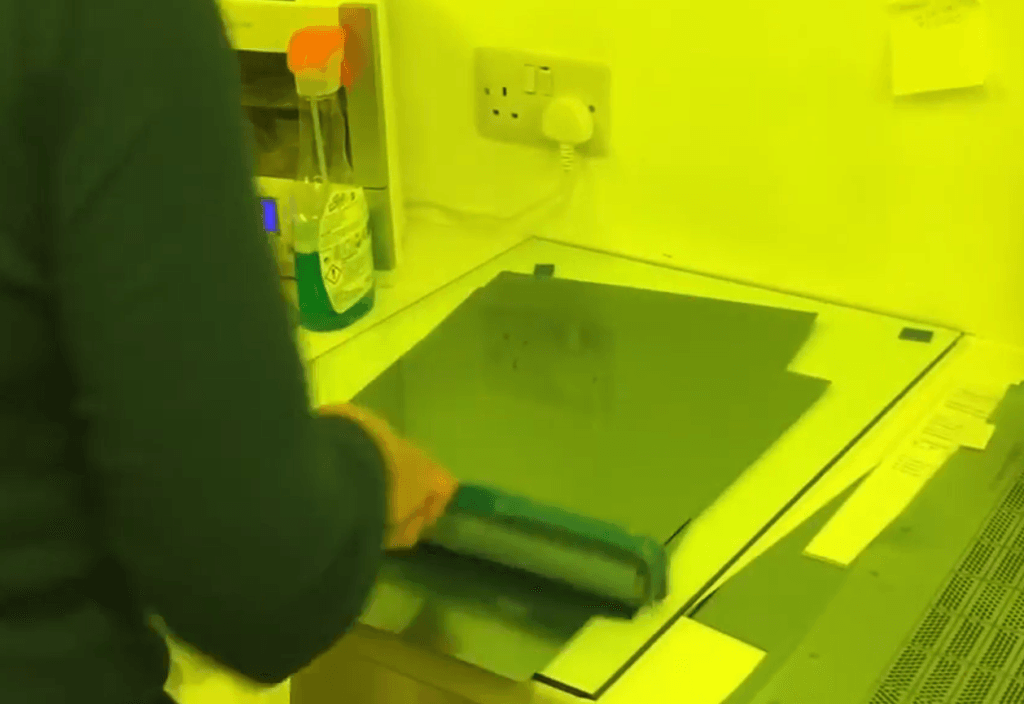
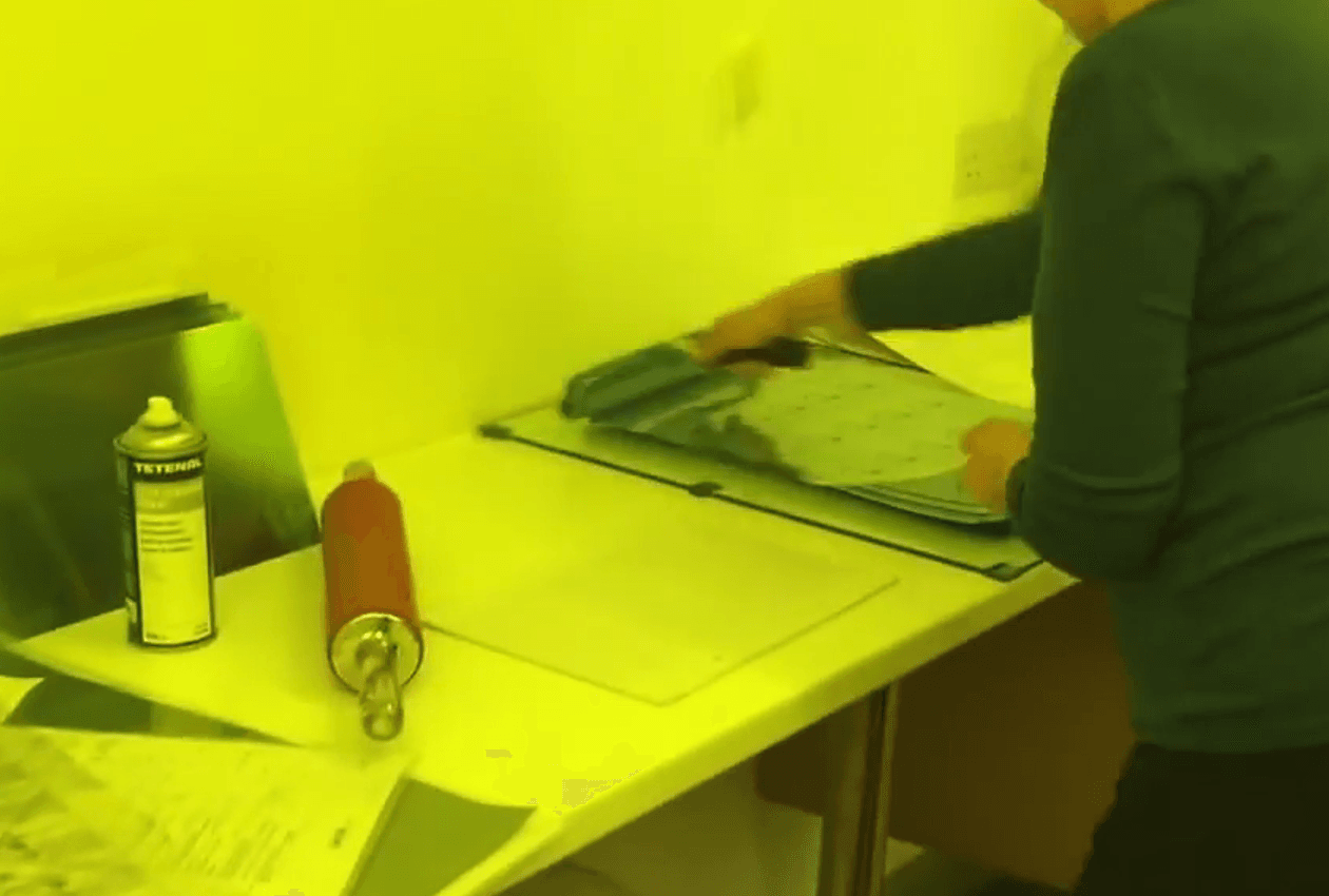
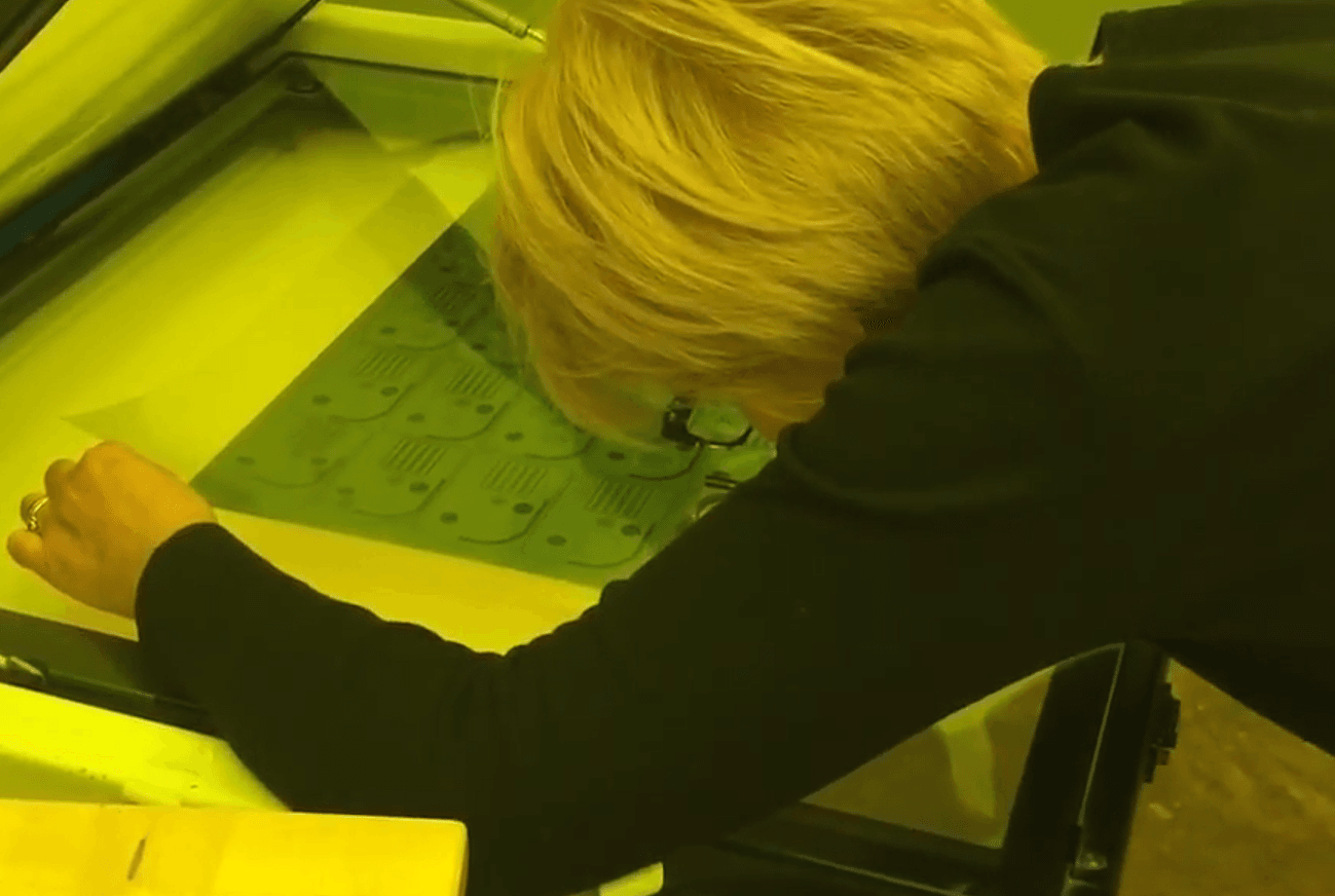
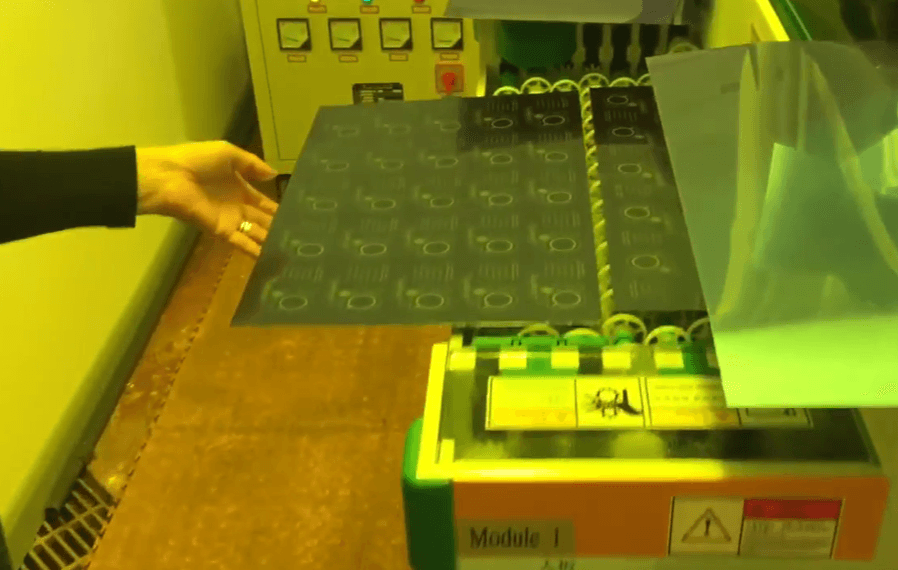
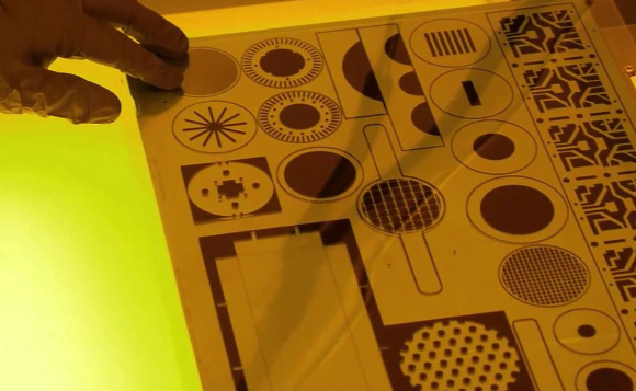
The chemical etching process for molybdenum begins by laminating the metal with a light-sensitive photoresist, which is then exposed to UV light to transfer the CAD image of the component. The unexposed photoresist areas are developed and removed, and the exposed metal is sprayed with specific etchant chemicals tailored for molybdenum to accurately remove the unprotected areas. Finally, the remaining photoresist is stripped away to reveal the finished etched component.

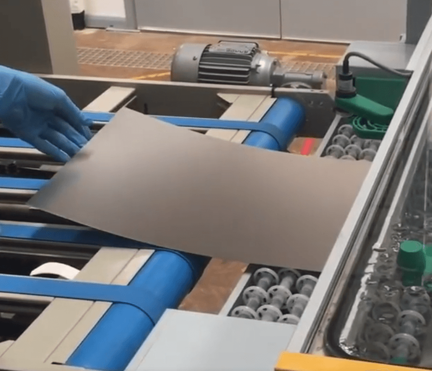
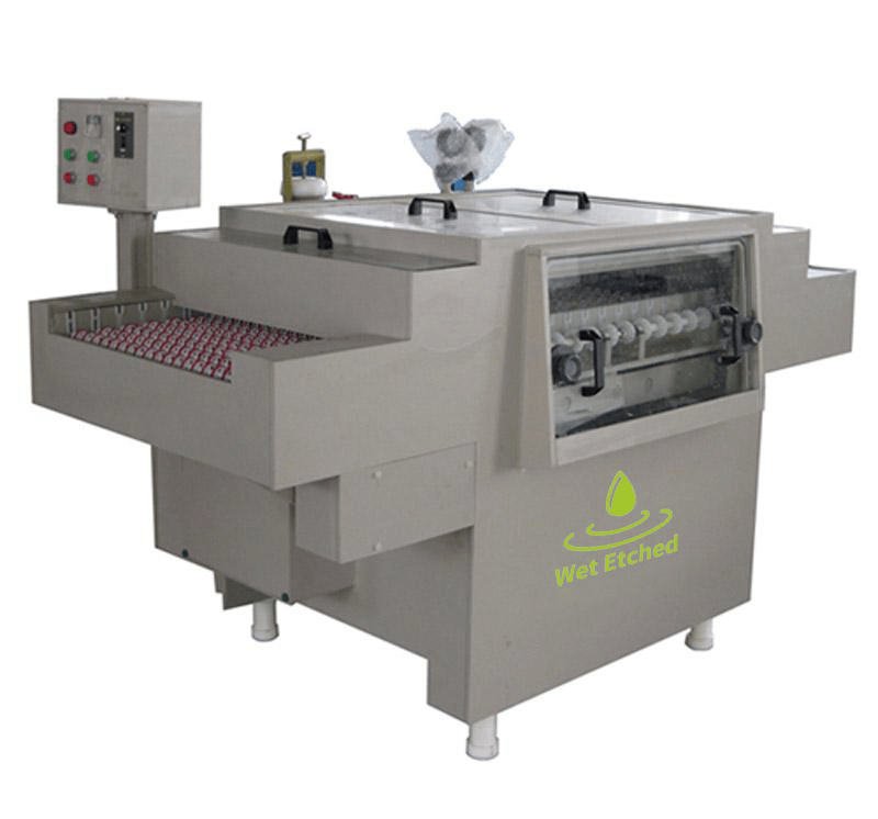
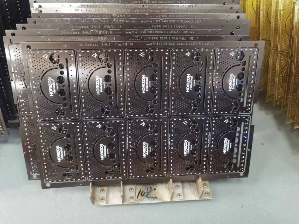
Wet Metal Etching Production workshop-  Shenzhen Xinxin Precision Equipment Co., Ltd.
Chemical etching Molybdenum Factory Process

Digital Tooling and Economic Efficiency

One of the key advantages of chemical etching molybdenum is its use of digital tooling. Unlike traditional methods that require expensive and difficult-to-adapt steel molds, digital tooling for etching is quick to adapt and change, often within an hour. This ensures that large quantities of products can be reproduced with zero tool wear, guaranteeing that the first and millionth part produced are exactly the same.

The adaptability of digital tooling makes it ideally suited for both prototype and high-volume production runs. This “risk-free” design optimization incurs no financial penalties and boasts a turnaround time that is estimated to be 90% quicker than for stamped parts, which also require substantial upfront investment in mold fabrication.

View our chemical etching Molybdenum process capabilities and pricing packages

[custom_pricing]

Applications of Etched Molybdenum Components

The chemical etching process is suitable for virtually any molybdenum component between 0.01mm and 1.5mm in thickness. Here are some examples where chemical etching molybdenum truly adds value:

Heat Shields and Thermal Management Components: Molybdenum’s high melting point and thermal stability make it ideal for components used in high-temperature environments. Chemical etching allows for the creation of intricate heat shields and thermal management components that can withstand extreme conditions without deforming or degrading.

Micro-Electromechanical Systems (MEMS): Molybdenum is often used in MEMS devices due to its mechanical properties and electrical conductivity. The precision of chemical etching is crucial for producing the fine features required in these miniature devices, ensuring reliability and performance in applications such as sensors and actuators.

Semiconductor Manufacturing: Molybdenum components are widely used in the semiconductor industry for their excellent performance in high-temperature and corrosive environments. Chemical etching provides the precision needed for fabricating components like targets for sputtering processes and components in chemical vapor deposition (CVD) systems.

Medical Devices: Due to its biocompatibility and strength, molybdenum is used in various medical devices. Chemical etching allows for the production of detailed and complex components necessary for medical implants and instruments, ensuring precision and safety.

Summary

Molybdenum exhibits a range of characteristics that make it ideal for numerous industrial applications. The chemical etching process offers significant advantages for producing complex and safety-critical molybdenum components, including:

  • No expensive hard tooling
  • Rapid transition from prototype to production
  • Almost unlimited part complexity
  • Burr- and stress-free component features
  • Unaffected metal properties
  • Suitability for all grades, with accuracy to ±0.025 mm
  • Lead times measured in days, not weeks or months

The versatility of chemical etching molybdenum, combined with WET Etched’s extensive experience, makes it a compelling option for manufacturing molybdenum components across diverse and demanding applications. This process stimulates innovation, removing obstacles inherent in traditional sheet metalworking technologies.

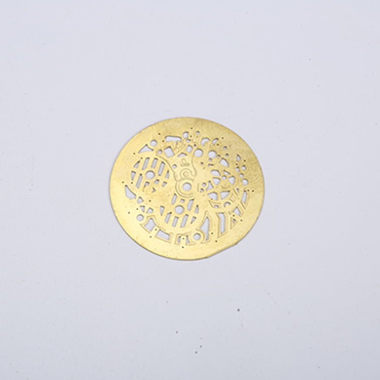
The Chemical Etching Brass Process: Precision and Innovation with WET Etched

The chemical etching process for brass creates precision components by selectively removing metal through a photoresist mask. This modern technique offers numerous inherent advantages over conventional sheet metalworking, including the ability to produce parts without degrading material properties since no force or heat is used during processing. It also allows for almost limitless part complexity, with component features machined simultaneously using etchant chemistries.

What is Chemical Etching Brass and How Does It Work?

Chemical etching brass is a metalworking process that uses corrosive chemicals to etch complex and precise components from brass. This process is highly favored in modern metal machining due to its high precision and low failure rate.

The chemical etching process for brass begins by laminating the metal with a light-sensitive photoresist, which is then exposed to UV light to transfer the CAD image of the component. The unexposed photoresist areas are developed and removed, and the exposed metal is sprayed with etchant chemicals to accurately remove the unprotected brass. Finally, the remaining photoresist is stripped away to reveal the finished etched component.

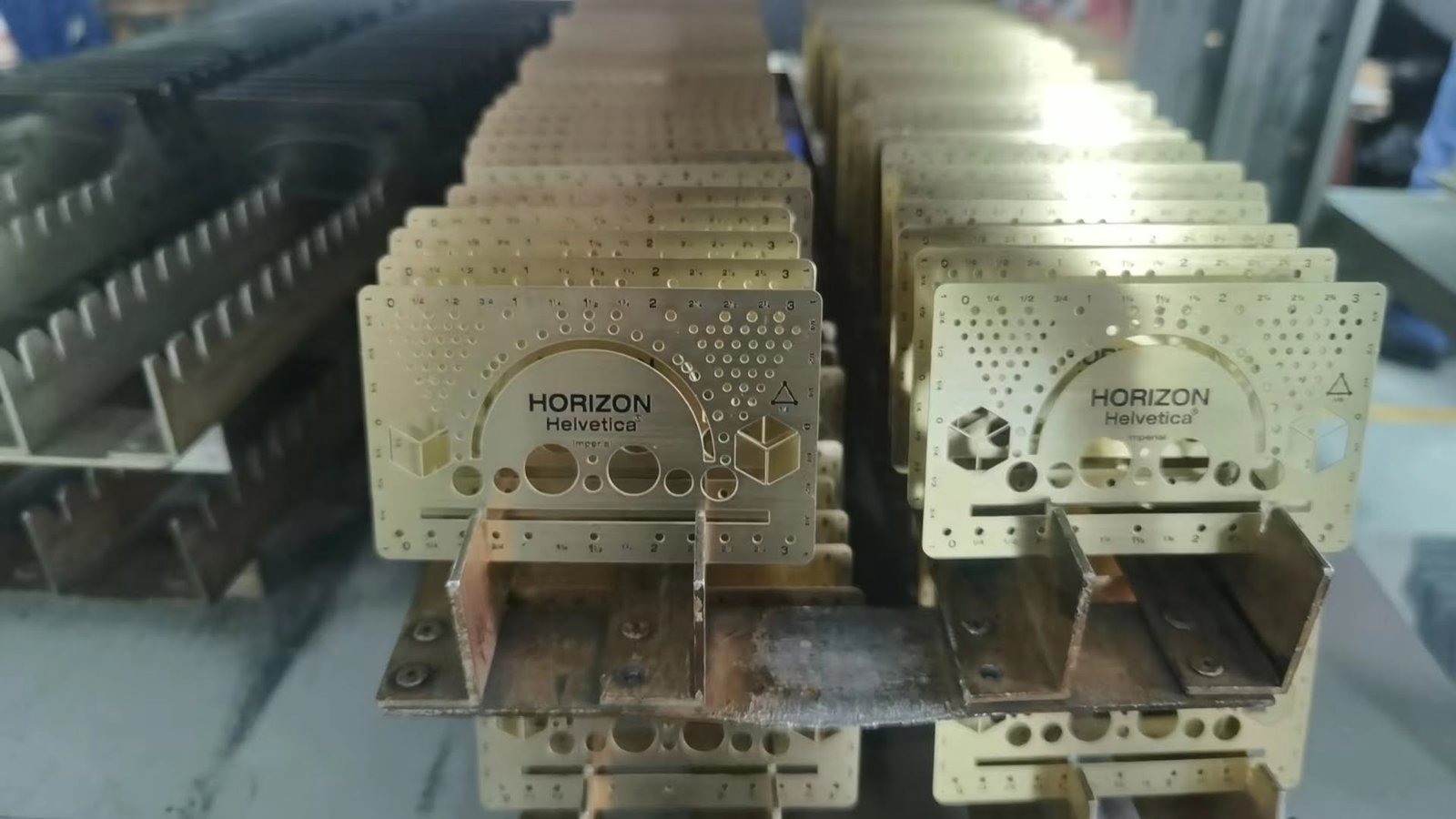
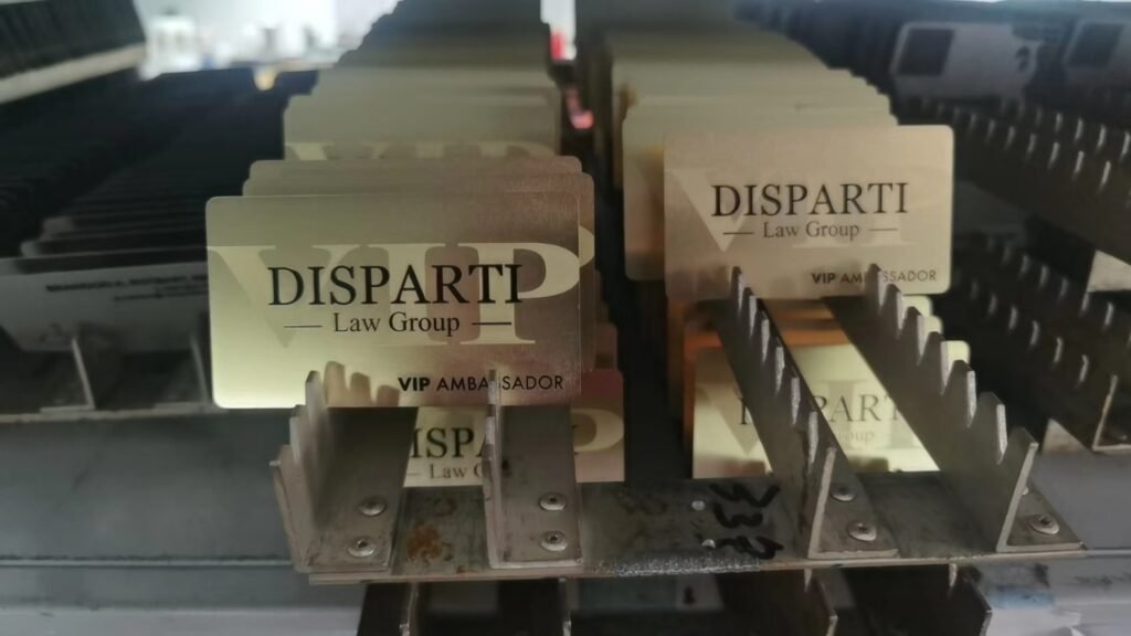
Wet Metal Etching Production workshop-  Shenzhen Xinxin Precision Equipment Co., Ltd.
Chemical etching brass Factory Process

Digital Tooling and Economic Efficiency

One of the key advantages of chemical etching brass is its use of digital tooling. Unlike traditional methods that require expensive and difficult-to-adapt steel molds, digital tooling for etching is quick to adapt and change, often within an hour. This ensures that large quantities of products can be reproduced with zero tool wear, guaranteeing that the first and millionth part produced are exactly the same.

The adaptability of digital tooling makes it ideally suited for both prototype and high-volume production runs. This “risk-free” design optimization incurs no financial penalties and boasts a turnaround time that is estimated to be 90% quicker than for stamped parts, which also require substantial upfront investment in mold fabrication.

View our chemical etching brass process capabilities and pricing packages

[custom_pricing]

Applications of Etched Brass Components

The chemical etching process is suitable for virtually any brass component between 0.01mm and 1.5mm in thickness. Here are some examples where chemical etching brass truly adds value:

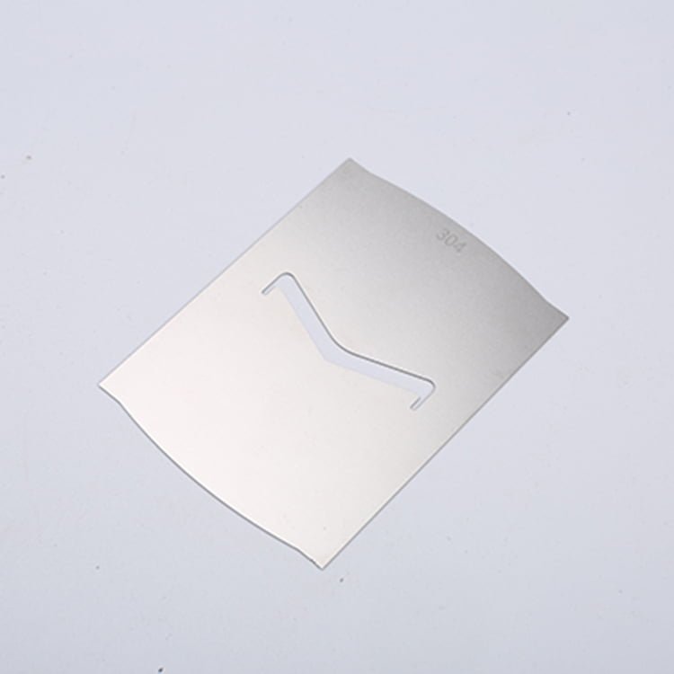
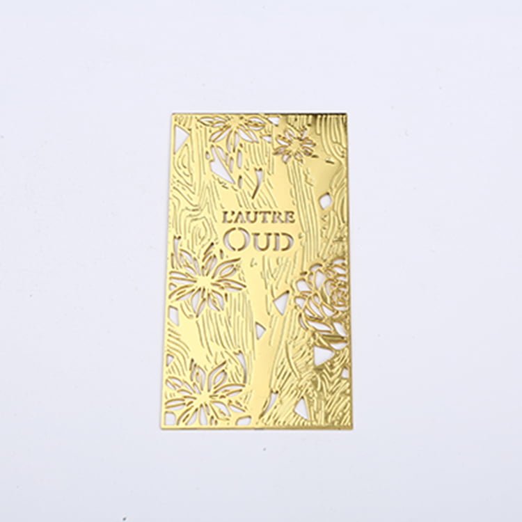
  • Bookmark Etching

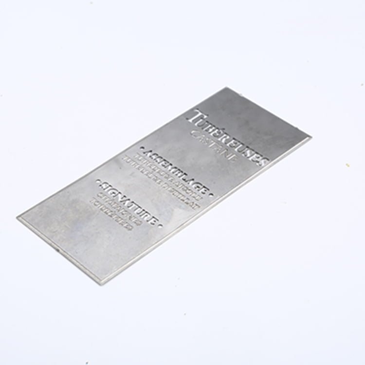
    Accurate etching of metal bookmarks, combining functionality with artistic design. View our etching production facility WET – Precision Etching Specialist

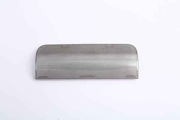
  • Car Door Sill Decorative Strip Etching

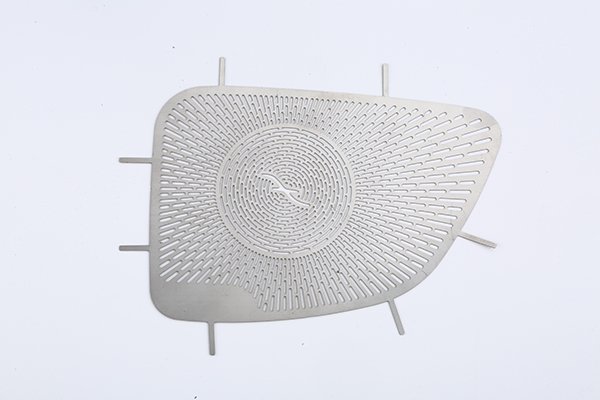
    Accurate etching of decorative strips for car door sills, enhancing the vehicle’s aesthetic appeal. View our etching production facility WET – Precision Etching Specialist

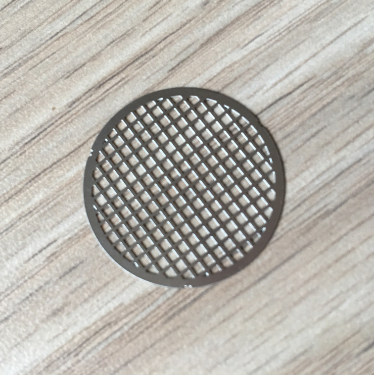
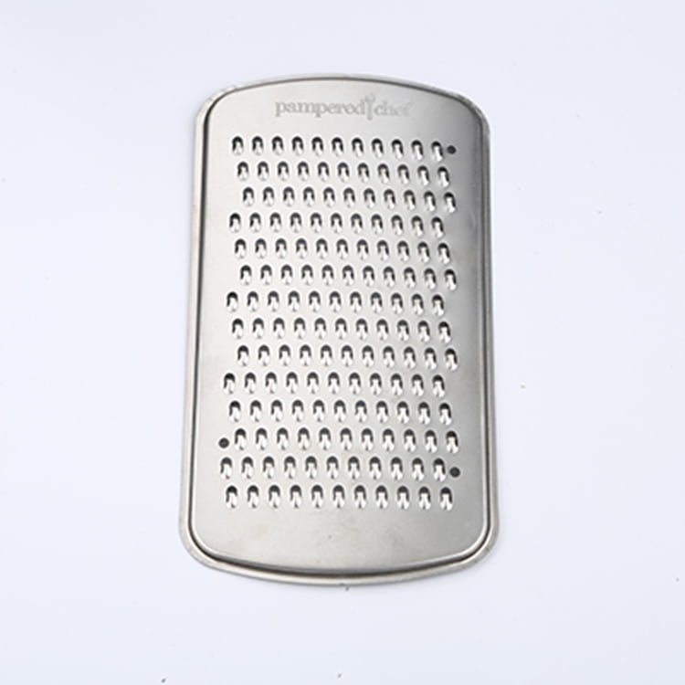
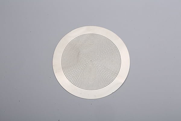
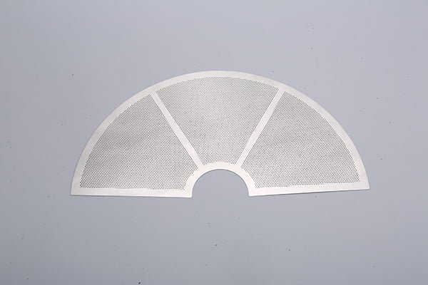
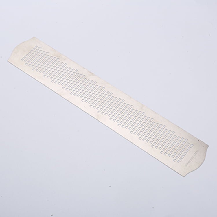
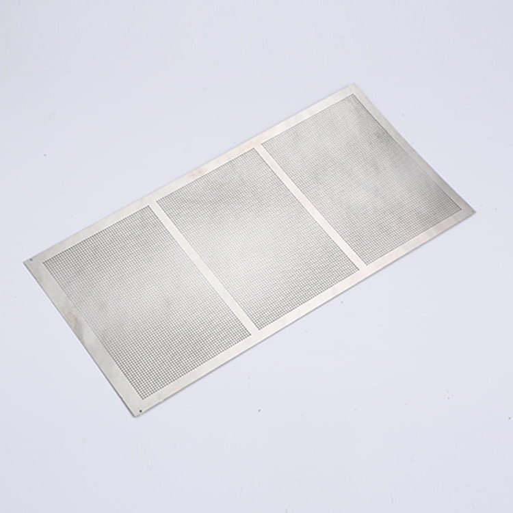
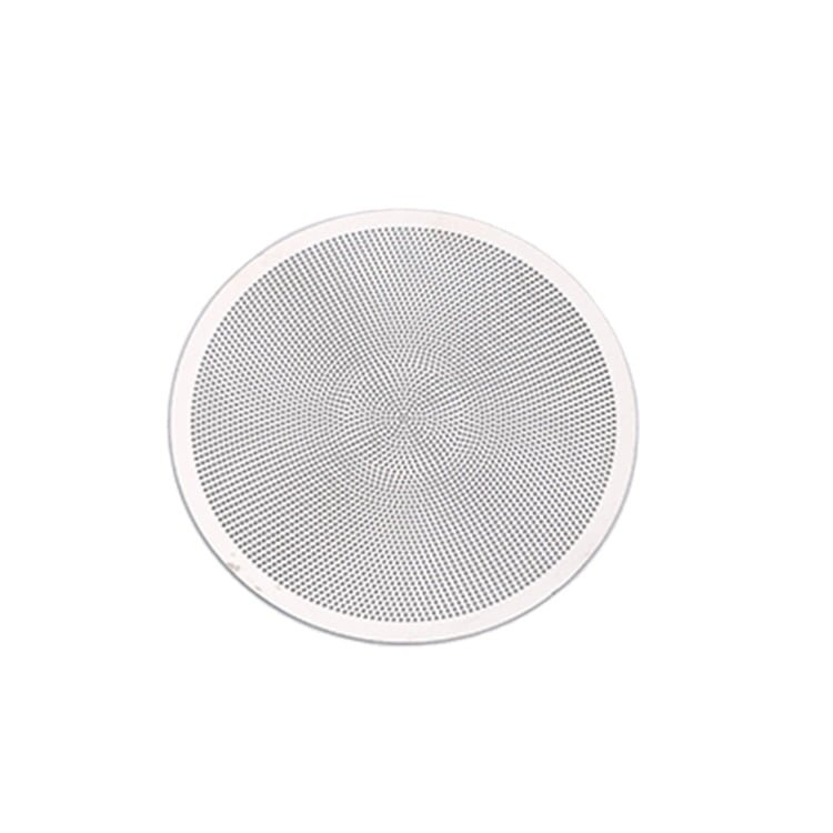
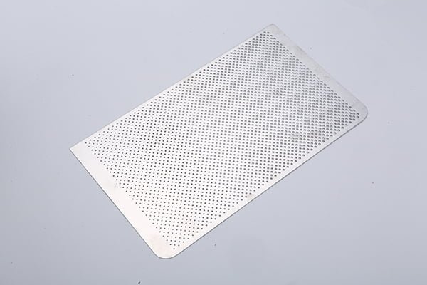
Meshes, Filters, and Sieves: Chemical etching offers greater levels of complexity when producing thin, precision brass meshes, filters, and sieves. Metal is removed simultaneously, allowing multiple aperture geometries to be incorporated without high tool or processing costs. Unlike punch-perforated sheets, photo-etched mesh is burr-free and stress-free, maintaining zero material degradation.

For example, a 150-micron thick precision brass mesh used in radiation detection devices is etched by WET Etched to precision tolerances below the standard ±10% material thickness. The critical honeycomb-shaped mesh array could not be economically produced by stamping due to the high investment required in press tooling, and laser cutting couldn’t achieve the necessary tolerances over such a large surface area.

Flexure Springs and Diaphragms: Often used in safety-critical or extreme environment applications, such as ABS braking systems, medical biosensors, or fuel injection systems, etched flexures can “flex” millions of times faultlessly. Chemical etching ensures that the fatigue strength of the brass is not altered, eliminating potential fracture sites and producing flexures free from burrs and recast layers.

Fuel Cell Bipolar Plates, Cooling Plates, and Fluidic Devices: Brass grades with specific properties are well-suited for fluidic devices used in liquid-to-liquid or liquid-to-gas heat exchangers, fuel cells, and cooling plates due to their excellent corrosion resistance. The complex grooves machined into these plates are well-suited to chemical etching, as they can be machined onto both sides in a single process without compromising flatness or introducing stresses and burrs.

Summary

Brass exhibits an array of characteristics that make it ideal for numerous industrial applications. The chemical etching process offers significant advantages for producing complex and safety-critical brass components, including:

  • No expensive hard tooling
  • Rapid transition from prototype to production
  • Almost unlimited part complexity
  • Burr- and stress-free component features
  • Unaffected metal properties
  • Suitability for all grades, with accuracy to ±0.025 mm
  • Lead times measured in days, not weeks or months

The versatility of chemical etching brass, combined with WET Etched’s extensive experience, makes it a compelling option for manufacturing brass components across diverse and demanding applications. This process stimulates innovation, removing obstacles inherent in traditional sheet metalworking technologies.

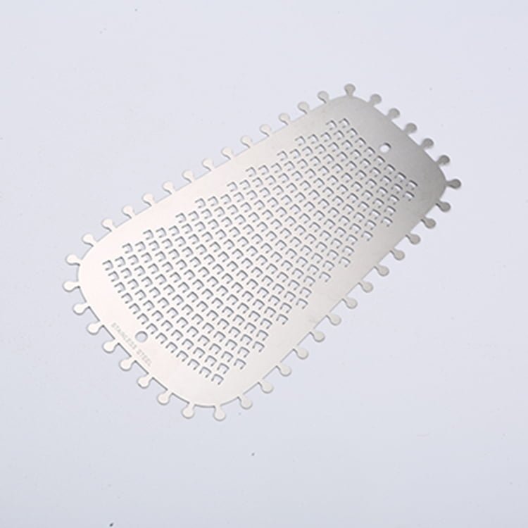
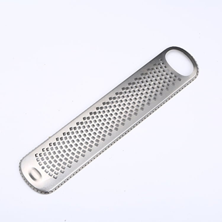
The Stainless Steel Chemical Etching Process

The stainless steel etching process creates precision components by selectively removing metal through a photoresist mask. This modern technique offers numerous inherent advantages over conventional sheet metalworking, including the ability to produce parts without degrading material properties since no force or heat is used during processing. It also allows for almost limitless part complexity, with component features machined simultaneously using etchant chemistries.

View or download our Photochemical Metal Etching White Paper How-to Guide

What is Stainless Steel Etching and How Does It Work?

Stainless steel etching is a metalworking process that uses corrosive chemicals to etch complex and precise components from stainless steel. This process is highly favored in modern metal machining due to its high precision and low failure rate.

The stainless steel etching process begins by laminating the metal with a light-sensitive photoresist, which is then exposed to UV light to transfer the CAD image of the component. The unexposed photoresist areas are developed and removed, and the exposed metal is sprayed with etchant chemicals to accurately remove the unprotected stainless steel. Finally, the remaining photoresist is stripped away to reveal the finished etched component.

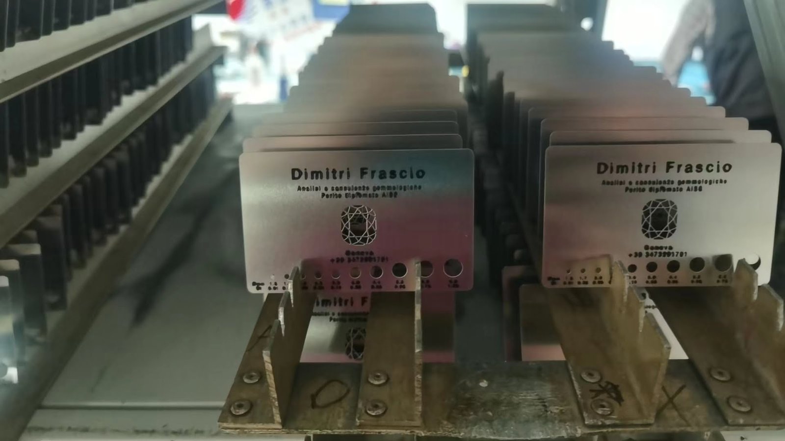
Wet Metal Etching Production workshop-  Shenzhen Xinxin Precision Equipment Co., Ltd.
Stainless Steel Etching Factory Process

Digital Tooling and Economic Efficiency

One of the key advantages of stainless steel etching is its use of digital tooling. Unlike traditional methods that require expensive and difficult-to-adapt steel molds, digital tooling for etching is quick to adapt and change, often within an hour. This ensures that large quantities of products can be reproduced with zero tool wear, guaranteeing that the first and millionth part produced are exactly the same.

The adaptability of digital tooling makes it ideally suited for both prototype and high-volume production runs. This “risk-free” design optimization incurs no financial penalties and boasts a turnaround time that is estimated to be 90% quicker than for stamped parts, which also require substantial upfront investment in mold fabrication.

View the chemical etching stainless steel workflow

Photo Wet Chemical Etching Process

Applications of Etched Stainless Steel Components

The stainless steel etching process is suitable for virtually any metal component between 0.01mm and 1.5mm in thickness. Here are some examples where stainless steel etching truly adds value:

Meshes, Filters, and Sieves: Chemical etching offers greater levels of complexity when producing thin, precision steel meshes, filters, and sieves. Metal is removed simultaneously, allowing multiple aperture geometries to be incorporated without high tool or processing costs. Unlike punch-perforated sheets, photo-etched mesh is burr-free and stress-free, maintaining zero material degradation.

For example, a 150-micron thick precision stainless steel mesh used in radiation detection devices is etched by WET Etched to precision tolerances below the standard ±10% material thickness. The critical honeycomb-shaped mesh array could not be economically produced by stamping due to the high investment required in press tooling, and laser cutting couldn’t achieve the necessary tolerances over such a large surface area.

Flexure Springs and Diaphragms: Often used in safety-critical or extreme environment applications, such as ABS braking systems, medical biosensors, or fuel injection systems, etched flexures can “flex” millions of times faultlessly. Chemical etching ensures that the fatigue strength of the steel is not altered, eliminating potential fracture sites and producing flexures free from burrs and recast layers.

Fuel Cell Bipolar Plates, Cooling Plates, and Fluidic Devices: Stainless steel grades with increased levels of chromium are well-suited for fluidic devices used in liquid-to-liquid or liquid-to-gas heat exchangers, fuel cells, and cooling plates due to their high corrosion resistance. The complex grooves machined into these plates are well-suited to chemical etching, as they can be machined onto both sides in a single process without compromising flatness or introducing stresses and burrs.

Summary

Stainless steel and its various grades possess characteristics that make them ideal for numerous industrial applications. The etching process offers significant advantages for producing complex and safety-critical stainless steel components, including:

  • No expensive hard tooling
  • Rapid transition from prototype to production
  • Almost unlimited part complexity
  • Burr- and stress-free component features
  • Unaffected metal properties
  • Suitability for all grades, with accuracy to ±0.025 mm
  • Lead times measured in days, not weeks or months

The versatility of stainless steel etching, combined with WET Etched’s extensive experience, makes it a compelling option for manufacturing stainless steel components across diverse and demanding applications. This process stimulates innovation, removing obstacles inherent in traditional sheet metalworking technologies.

Fine tungsten probe batch customization manufacturer

WET is a professional manufacturer of high-quality tungsten probes for batch customization. In the realm of precision engineering, where every micron matters, fine tungsten probes emerge as indispensable tools driving innovation and discovery. As manufacturers strive to meet the exacting demands of various industries, the role of fine tungsten probe batch customization becomes paramount.

ParameterDescriptionTypical RangeApplication Areas
Probe Tip DiameterDiameter of the probe tip0.001 – 0.020 inchesPrecision Instrument Probes, Microelectronics
Tip RadiusRadius of the probe tip0.0005 – 0.005 inchesSemiconductor Testing, Nanotechnology
Taper LengthLength of the taper portion0.010 – 0.200 inchesBiomedical Research, DNA Sequencing
Overall LengthTotal length of the tungsten probe0.050 – 1.000 inchesElectronics Testing, Material Analysis
Shaft DiameterDiameter of the probe shaft0.005 – 0.050 inchesMEMS (Microelectromechanical Systems)
CoatingOptional coating for enhanced propertiesVarious options availableOptoelectronics, Optical Fiber Testing
Common tungsten needle probe custom specifications

Detailed Application Areas:

  1. Precision Instrument Probes: Tungsten probes with precise tip diameters and tip radii are commonly used for probing and testing delicate instruments and components in precision engineering applications.
  2. Microelectronics: Tungsten probes find extensive use in the microelectronics industry for testing integrated circuits, probing microchips, and analyzing semiconductor materials.
  3. Semiconductor Testing: Tungsten probes with sharp tip radii are essential for semiconductor testing, where they enable precise probing of small features on silicon wafers and other semiconductor substrates.
  4. Nanotechnology: Tungsten probes with ultrafine tip radii are indispensable tools in nanotechnology research, enabling scientists to manipulate and characterize nanoscale structures with unparalleled precision.
  5. Biomedical Research: Tungsten probes with specialized coatings and precise tip geometries are utilized in biomedical research for applications such as cellular probing, electrophysiology, and neurostimulation.
  6. DNA Sequencing: Tungsten probes are employed in DNA sequencing applications, where they facilitate the manipulation and analysis of DNA molecules with high precision and accuracy.
  7. Electronics Testing: Tungsten probes are used in various electronics testing applications, including printed circuit board (PCB) testing, device characterization, and failure analysis.
  8. Material Analysis: Tungsten probes are utilized in material analysis applications such as scanning electron microscopy (SEM), atomic force microscopy (AFM), and surface profilometry for precise surface characterization and analysis.
  9. MEMS (Microelectromechanical Systems): Tungsten probes play a crucial role in MEMS fabrication and testing, where they enable precise probing and manipulation of microscale structures and devices.
  10. Optoelectronics: Tungsten probes are used in optoelectronics applications for testing and characterizing optical components, photonic devices, and fiber-optic systems.

If you have Custom tungsten needles, please feel free to contact us.

    FAQs

    [FAQS]

    Crafting Precision: The Art of Fine Tungsten Probe Manufacturing

    Crafting fine tungsten probes is a symphony of precision and expertise. Beginning with meticulously sourced tungsten materials, manufacturers employ advanced manufacturing techniques to transform raw materials into intricate probes. Through a series of refining processes, including precision grinding, shaping, and polishing, each probe is meticulously crafted to meet the highest standards of accuracy and durability.

    Tailored to Perfection: The Importance of Batch Customization

    In today’s fast-paced industries, where unique applications demand tailored solutions, batch customization emerges as a game-changer. Manufacturers of fine tungsten probes recognize the diverse needs of their clientele and offer bespoke solutions to meet specific requirements. Whether it’s adjusting the tip radius, length, or shape of the probe, customization ensures that each batch of probes is perfectly suited to its intended application.

    Precision Meets Performance: Applications of Customized Tungsten Probes

    The applications of customized tungsten probes span a myriad of industries, from semiconductor manufacturing and electronics testing to biomedical research and beyond. In the semiconductor industry, customized probes play a crucial role in probing and testing integrated circuits with unparalleled precision. In biomedical research, they enable scientists to explore the intricate world of cellular biology and nanotechnology, driving breakthrough discoveries and innovations.

    The Future of Precision Engineering: Innovations in Tungsten Probe Customization

    As technology advances and industries evolve, the future of precision engineering holds boundless possibilities. Innovations in materials science, manufacturing techniques, and customization capabilities promise to elevate the performance and versatility of tungsten probes to new heights. From nano-scale probing to space exploration, customized tungsten probes are poised to redefine the boundaries of precision engineering and shape the future of innovation.

    Partnering for Precision: Choosing the Right Manufacturer

    In the quest for precision, choosing the right manufacturer is paramount. When selecting a partner for fine tungsten probe customization, look for a company with a proven track record of expertise, reliability, and customer satisfaction. By partnering with a trusted manufacturer, you can unlock the full potential of customized tungsten probes and propel your projects to new levels of accuracy and performance.

    Custom Tungsten Needles

    In the wave of modern technological advancements, the demand for precision machining is steadily rising. From microelectronic components to medical devices, there’s an ever-growing need for highly precise tools and parts. Leading the charge in this arena is WET High Precision Metal Machining Company, specializing in crafting super-precise tungsten needles with a minimum tip radius of just 0.001 inches.

    For medical

    Hook-type 99.5% tungsten needle

    These miniature precision microtool tips are helpful for particle manipulation or sample prep. They are available as individual interchangeable tips.

    Tungsten alloy with durable 0.001″ radius tip

    90° Microhook 99.5% tungsten

    These miniature precision microtool tips are helpful for particle manipulation or sample prep. They are available as individual interchangeable tips.

    99.5% tungsten Microneedle – Straight

    These miniature precision microtool tips are helpful for particle manipulation or sample prep. They are available as individual interchangeable tips. 

    Industrial use (laboratory, etc.)

    In addition, we can also perform custom threading on tungsten needles.

    Thread SizeThread Diameter (mm)Pitch (mm)
    M33 mm0.5 mm
    M3.53.5 mm0.6 mm
    M44 mm0.7 mm
    M55 mm0.8 mm
    M66 mm1 mm
    M88 mm1.25 mm
    M1010 mm1.5 mm
    M1212 mm1.75 mm
    M1414 mm2 mm
    M1616 mm2 mm
    M1818 mm2.5 mm
    M2020 mm2.5 mm
    M2222 mm2.5 mm
    M2424 mm3 mm
    M2727 mm3 mm
    M3030 mm3.5 mm
    Threaded tungsten needle customization

    Crafting tungsten needles is a complex and highly precise art. It requires specialized expertise and cutting-edge equipment to ensure every needle meets the highest standards. At WET, we boast extensive experience and leading-edge technology to meet even the most stringent demands of our clients.

    If you have Custom tungsten needles, please feel free to contact us.

      FAQs

      [FAQS]

      Our strength lies in our ability to offer customized solutions. Whether it’s the size of the tip radius or the length and shape of the needle, we can tailor our products to fit our clients’ exact specifications. This personalized service allows us to cater to the diverse needs of various industries, providing our clients with optimal solutions.

      In addition to customization, we prioritize quality control. Throughout the production process, we maintain strict control over every step to ensure each needle meets the highest quality standards. Employing advanced inspection equipment and techniques, we conduct precise testing on each needle to ensure its accuracy and stability.

      Furthermore, we value communication and collaboration with our clients. We remain open-minded, listening to our clients’ needs and feedback, continuously improving and optimizing our products and services. We understand that customer satisfaction is our greatest motivation, so we are committed to providing exceptional products and services.

      Custom tungsten needles are one of WET High Precision Metal Machining Company’s core competencies. With our wealth of experience, leading-edge technology, and top-notch service, we can meet our clients’ various needs for super-precise tungsten needles. Whether in electronics, medical, aerospace, or other fields, we can provide our clients with the best solutions to help them achieve greater success. If you have any inquiries or questions about our products or services, please don’t hesitate to contact us. We are here to serve you wholeheartedly.

      Understanding Semiconductor Etching

      Semiconductor etching is a crucial step in the fabrication of electronic devices, allowing for the precise removal of material layers from semiconductors. This process is instrumental in creating the intricate patterns necessary for the functioning of integrated circuits.

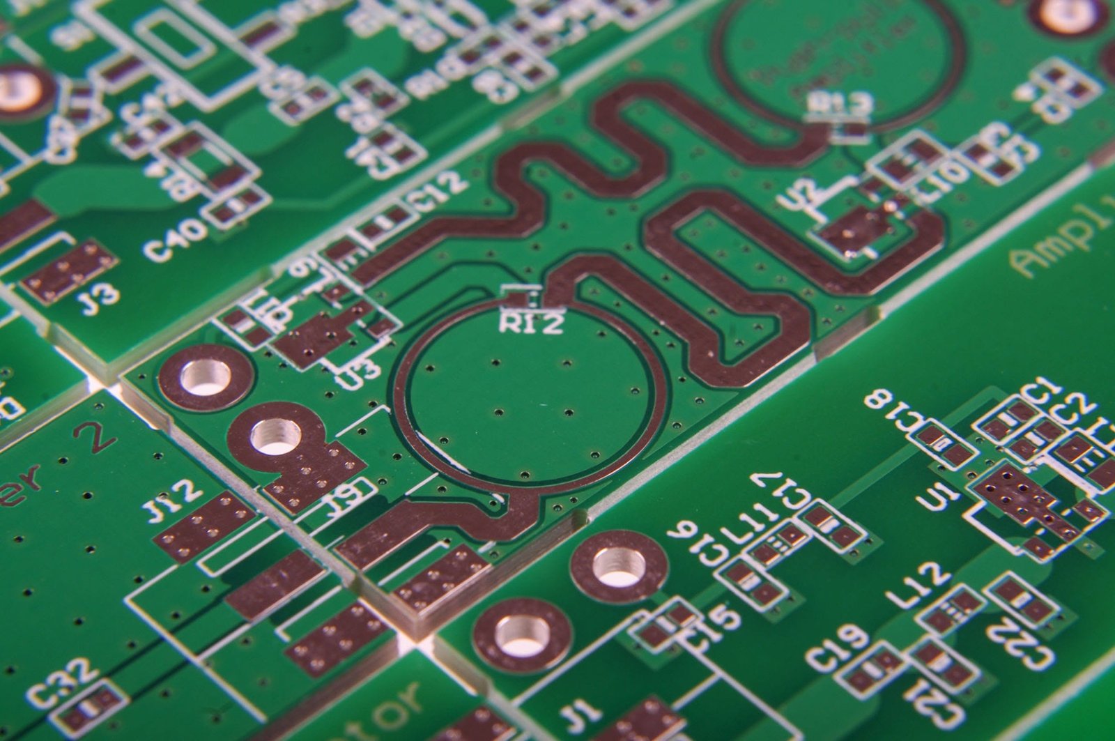
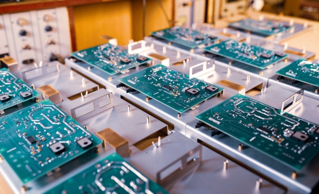
      If you want to produce PCBs, or semiconductors independently. Then I will disabuse you of the idea, because trying to produce PCBs or semiconductors complete and independently, I don’t think any company can afford the investment cost.

      Let’s start simply by understanding the PCB fabrication process.

      If you want to produce your own pcb's, then you need this equipment - PCB equipment list
      If you want to produce your own pcb’s, then you need this equipment – PCB equipment list

      1. Semiconductor Etching Equipment:

      1.1 LDI High-Precision Exposure Machine: The LDI (Laser Direct Imaging) high-precision exposure machine plays a vital role in the semiconductor etching process. This equipment uses laser technology to selectively expose photoresist-coated semiconductor wafers, defining the patterns that will guide the subsequent etching steps. LDI machines offer exceptional precision, enabling the production of intricate and miniaturized semiconductor components.

      1.2 Chemical Etching Equipment: Chemical etching equipment is designed to selectively remove material layers from semiconductor wafers. Among the common types are wet chemical etching and dry etching systems.

      • Wet Chemical Etching:
        • Equipment Overview: Wet chemical etching involves immersing the semiconductor wafer in a chemical solution to selectively remove material.
        • Role: The equipment facilitates controlled material removal, allowing for the creation of precise patterns.
        • Common Equipment: Manufacturers such as Dragon Etching provide wet chemical etching systems, ensuring uniform and controlled etching processes.
      • Dry Etching Systems:
        • Equipment Overview: Dry etching, including techniques like reactive ion etching (RIE) and plasma etching, employs gases and plasmas to remove material.
        • Role: These systems offer high-precision etching with minimal damage to the underlying material.
        • Common Equipment: Oxford Instruments is a reputable manufacturer of dry etching systems, providing solutions for various semiconductor materials.

      2. Common Etchants in Semiconductor Etching:

      Analyzing several common etchants is crucial to understanding their application and parameters. Below is a table summarizing some commonly used etchants:

      EtchantCompositionSelectivityTemperature (°C)Etch Rate (nm/min)
      Buffered HFHF + NH4FHighAmbient~1 – 10
      Piranha SolutionH2SO4 + H2O2ModerateAmbientVariable
      KOHKOHHigh~50 – 80~50 – 100
      SF6 PlasmaSF6 + O2High~50 – 100~10 – 100
      Semiconductor etchant

      3. Basic Applications of Semiconductor Etching:

      The semiconductor etching process finds applications in various industries, including:

      • Glass Etching: Used for creating microstructures on glass surfaces.
      Glass Etching
      • Silicon Wafer Etching: Critical in the production of integrated circuits.
      Semiconductor etch
      • MEMS (Micro-Electro-Mechanical Systems): Enables the fabrication of miniature mechanical components on semiconductor wafers.
      MEMS (Micro-Electro-Mechanical Systems)

      Semiconductor Etching Process Flow:

      3.1. Photoresist Application:

      • A thin layer of photoresist is applied to the semiconductor wafer.

      3.2. Exposure:

      • The LDI high-precision exposure machine selectively exposes the photoresist to define the desired patterns.

      3.3. Development:

      • The exposed photoresist is developed, revealing the pattern on the semiconductor surface.

      3.4. Etching:

      • The semiconductor wafer undergoes wet or dry etching, selectively removing material based on the developed pattern.

      3.5. Resist Stripping:

      • Any remaining photoresist is removed, leaving behind the etched semiconductor pattern.

      Semiconductor etching is a sophisticated process with a range of specialized equipment and etchants, crucial for the production of advanced electronic devices. Understanding the intricacies of this process is essential for achieving precision and efficiency in semiconductor fabrication.

      If you have PCB or semiconductor processing in mind, please do not hesitate to contact us. Contact us today. We will provide you with processing and manufacturing services. All you need to do is provide us with the appropriate drawings.

        Unveiling the Versatile Applications of Wet Etching in Diverse Fields

        Wet etching is a dynamic and versatile process, playing a pivotal role in a wide range of application areas. From microelectromechanical systems (MEMS) to semiconductor manufacturing, solar cell production, microfluidics, and photolithography, wet etching offers its unique solutions. In this article, we’ll explore the fascinating world of wet etching in different fields, delving into its diverse applications, specific needs, and the challenges it addresses. By the end of this read, you’ll have a comprehensive understanding of the profound impact of wet etching across multiple domains.

        Microelectromechanical Systems (MEMS) Wet Etching

        MEMS wet etching is an essential process in MEMS fabrication, where tiny mechanical and electronic devices are created. These devices, often used in sensors, actuators, and more, rely on wet etching to define their structures.

        Semiconductor Wet Etching

        In the world of semiconductor manufacturing, wet etching is a cornerstone process. It is used to define circuit patterns, remove unwanted layers, and shape intricate features on semiconductor wafers.

        Solar Cell Wet Etching

        Solar cell production relies on wet etching to texture the surface of solar panels, enhancing light absorption and overall energy efficiency. This is a key step in creating effective photovoltaic cells.

        Microfluidic Wet Etching

        Microfluidics is a cutting-edge field with applications in healthcare, chemistry, and biology. Wet etching is used to create intricate microchannels and structures for precise fluid control.

        Photolithography Wet Etching

        Photolithography is a fundamental technique in microfabrication. Wet etching is employed to define patterns in a photoresist, transferring these patterns onto the underlying material.

        • For a detailed explanation of photolithography wet etching, refer to this SPIE article.

        Addressing Unique Needs and Challenges

        Wet etching is an art that requires a deep understanding of materials, etchants, and process control. Each application area presents its own set of challenges. The choice of etchant, temperature control, and etching time are just a few of the variables that must be considered.

        • In semiconductor manufacturing, precision and selectivity are paramount.
        • In solar cell production, the focus is on enhancing light capture.
        • Microfluidics demands intricate microchannel fabrication.
        • Photolithography requires precise pattern transfer.

        These varying needs and challenges underscore the importance of expertise and innovation in wet etching processes tailored to each application.

        Wet etching is more than just a materials processing technique; it’s a transformative force across multiple fields. From MEMS and semiconductor manufacturing to solar cell production, microfluidics, and photolithography, wet etching continues to reshape technology and science. By understanding its applications, unique requirements, and challenges, we can fully appreciate the profound impact it has on our world.

        As technology and science advance, wet etching will undoubtedly find new applications and continue to push the boundaries of what is possible in each of these exciting fields.

        Exploring the Impact of Wet Corrosion on a Variety of Materials

        Wet etching is a fundamental process in materials science and engineering. Its impact on various materials, from silicon to copper, glass, gold, silicon nitride, sapphire, tungsten, and metals, is both profound and diverse. In this article, we will delve into the world of wet etching and its effects on these materials. We’ll discuss the importance of selecting the correct etching method and share insights on how to navigate wet etching challenges for different materials. By the end of this article, you’ll have a comprehensive understanding of the complex relationship between wet etching and different materials.

        Understanding Wet Etching

        Wet etching is a chemical process that selectively removes material from a substrate by immersing it in a chemical solution. Its effects on various materials are intriguing and often require careful consideration.

        Learn about the metals we can etch and the etching methods.

        Effects on Silicon

        Silicon is a commonly used semiconductor material. Wet etching can precisely shape silicon, making it a critical process in microfabrication. The wet etching of silicon is an area of extensive research and development.

        Implications for Copper

        Wet etching can be a powerful tool in the electronics industry. For instance, it plays a role in the fabrication of printed circuit boards (PCBs), where copper layers must be etched to create intricate circuit patterns. Learn more about copper etching.

        Wet Etching of Glass

        Glass is another fascinating material when it comes to wet etching. Understanding the wet etching of glass is crucial for applications like microfluidics and optical components.

        Gold and Its Properties

        Gold, known for its chemical stability, can be etched using various wet etching techniques. This process is significant in creating gold-based microelectrodes for biological and electronic applications. Explore gold etching methods.

        Wet Etching of Silicon Nitride

        Silicon nitride is a material often used in microelectronics and MEMS. Wet etching of silicon nitride is complex and requires precise control. Learn about silicon nitride wet etching.

        Effects on Sapphire

        Sapphire, prized for its hardness and optical properties, is used in various applications. Wet etching plays a role in shaping sapphire for optical components. Discover the intricacies of sapphire etching.

        Tackling Wet Etching of Tungsten

        Tungsten, a material with high melting and boiling points, is a vital component in electronics. Understanding wet etching of tungsten is essential for device fabrication.
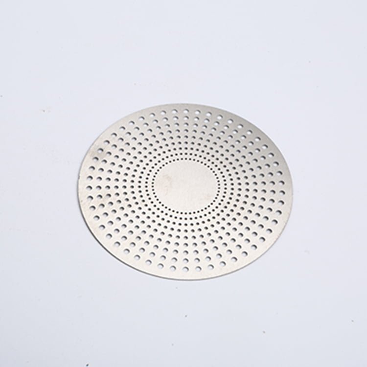
        Etching Various Metals

        The wet etching of metals is a diverse field, as each metal behaves differently in various etchants. Explore the etching of different metals to appreciate the nuances.
        Choosing the Right Etching Method

        Selecting the correct wet etching method is crucial to achieving the desired results. Parameters such as the choice of etchant, etch rate, and etch selectivity must be considered.

        Factors to Consider

        • Etching solutions
        • Temperature control
        • Etching time
        • Masking techniques
        • Safety precautions

        Wet etching is a versatile and valuable process in materials engineering. Its effects on different materials, from silicon to metals, are profound and often lead to innovative solutions in technology and manufacturing. By understanding the intricacies of wet etching and choosing the right method for the material at hand, engineers and researchers can unlock the full potential of this essential technique.

        Watch this video for a visual overview of Wet Etching Techniques.

        As the world of materials science and technology continues to advance, the relationship between wet etching and materials will undoubtedly yield more discoveries and applications, shaping the future of innovation.

        Understanding Wet Etching and Dry Etching in Semiconductor Fabrication

        The semiconductor industry is a complex web of processes, each playing a vital role in shaping the technology we use every day. Among these processes, etching stands out as a crucial step in defining and patterning various semiconductor components. In this article, we will unravel the intricacies of two primary etching methods – wet etching and dry etching – exploring how they work, their advantages, disadvantages, and specific applications. By the end of this read, you’ll possess a comprehensive understanding of these techniques and their pivotal role in semiconductor manufacturing.

        Wet Etching: A Chemical Approach

        Wet etching, also known as chemical etching, is a chemical process used extensively in semiconductor manufacturing. This method involves immersing a semiconductor wafer into a chemical solution to selectively remove specific layers or materials. Let’s dissect the fundamental aspects of wet etching:

        How Wet Etching Works:

        Wet etching relies on chemical reactions to remove unwanted materials from the semiconductor surface. A common technique within this category is chemical wet etching, where the composition of the chemical solution is carefully tailored to dissolve the target material while leaving the rest of the wafer untouched. For a more in-depth understanding, refer to this article on Chemical Etching.

        Anisotropic vs. Isotropic Wet Etching:

        Within wet etching, there are two fundamental categories – anisotropic and isotropic wet etching. Anisotropic etching removes material preferentially in one direction, resulting in sharply defined features, while isotropic etching removes material uniformly in all directions, yielding rounded features. For a visual representation, watch this informative video on Anisotropic and Isotropic Etching.

        Advantages and Disadvantages of Wet Etching:

        Wet etching offers precise control over etch depth and selectivity, making it suitable for intricate semiconductor structures. However, it has its drawbacks, such as limited control over lateral etching and the need for specialized chemical solutions.

        Dry Etching: The Physical Approach

        Dry etching, in contrast to wet etching, is a physical process that employs plasma or reactive gases to remove material from the wafer surface. Here’s a deeper dive into dry etching:

        How Dry Etching Works:

        Dry etching utilizes various techniques, such as reactive-ion etching (RIE) and inductively coupled plasma (ICP) etching, where a combination of gases and high-energy ions selectively etches the semiconductor material. For a detailed exploration of these techniques, refer to this scholarly article on RIE and ICP Etching.

        Advantages and Disadvantages of Dry Etching:

        Dry etching allows for precise control over etch profiles and high aspect ratios, minimizing lateral etching. However, it can be more expensive due to the equipment required and can pose challenges related to uniformity.

        Applications of Wet Etching and Dry Etching

        Semiconductor manufacturers often choose between wet etching and dry etching based on the specific requirements of their processes. Here are some key applications for each:

        • Wet Etching: Commonly used in MEMS (Micro-Electro-Mechanical Systems) fabrication, wet etching is ideal for applications where precise control over feature shapes is crucial.
        • Dry Etching: It finds its place in fabricating integrated circuits, microprocessors, and memory devices, where high aspect ratios and fine features are necessary.

        Understanding the principles of wet etching and dry etching is essential in the semiconductor industry, as it influences the success and precision of fabrication processes. Each method has its unique strengths and weaknesses, and the choice between them depends on the specific needs of the semiconductor device being manufactured.

        As semiconductor technology continues to advance, these etching techniques will evolve, offering even greater precision and control. To gain a glimpse into the future of semiconductor etching, watch this informative video on The Future of Semiconductor Etching.

        By exploring wet etching and dry etching in detail, you’re now better equipped to navigate the intricacies of semiconductor fabrication. Whether you’re a professional in the field or simply intrigued by the world of microelectronics, this knowledge empowers you to appreciate the marvels of modern technology.

        Guide to Drawing Standard Etching Design

        Wet etching is a fundamental process in microfabrication, allowing precise material removal to create intricate patterns and structures on substrates. The success of wet etching hinges on a series of design criteria that engineers and scientists must meticulously consider. In this blog, we will explore the key design criteria for wet etching, focusing on assumptions, dimensions, and the importance of hole size in achieving the desired results.

        Design Criteria for Wet Etching

        1. Assumptions Matter: Before delving into the design criteria, it’s crucial to set the right assumptions. For instance, in the case of wet etching, we assume a specific thickness. For the purpose of this discussion, let’s consider a thickness ranging from 0.1mm.
        2. Etching design formulas versus material thickness: Assuming a material thickness of 0.1mm, one of the first design criteria to consider is the hole diameter. To ensure proper etching, it’s often recommended to make the hole slightly larger than the material thickness. In this case, 1.2 times the material thickness would be 0.1mm * 1.2 = 0.12mm. Therefore, if the material thickness is 0.1mm, the hole should be designed to have a diameter of at least 0.12mm.
        3. Material Choice: The choice of material plays a significant role in wet etching. Different materials react differently to etchants. Engineers must select materials that are compatible with the chosen etchant to ensure a successful process.
        4. Hole Size Matters: The size of the holes created during wet etching is a critical design criterion. Smaller holes may lead to incomplete material removal, while larger holes may compromise structural integrity. Typically, materials with a thickness of 100μm or less can accommodate holes with a diameter of 0.12mm or more. Larger holes often result in more aesthetically pleasing and structurally sound outcomes.
        5. Alignment and Precision: Achieving precise alignment of the etched features is vital. Design drawings should incorporate alignment markers or registration features to ensure accurate positioning during the etching process. This is particularly crucial when dealing with multilayer structures or when specific patterns must be aligned with pre-existing features.
        6. Minimum Feature Size: It’s advisable to establish a minimum feature size for your design drawings. For instance, it’s generally recommended that no marked details be smaller than 0.1mm. This corresponds to 100μm. Maintaining a minimum feature size helps ensure that the etching process can accurately replicate the desired patterns and structures without the risk of incomplete or distorted etching.
        7. Quality Control and Inspection: Design criteria should include provisions for quality control and inspection during and after the wet etching process. This involves specifying methods and tools for verifying that the final product meets the intended design specifications. Inspection processes may include optical microscopy, surface profilometry, or other measurement techniques to validate critical dimensions and surface finish.

        Conclusion

        Wet etching is a precise and versatile process used in microfabrication and nanotechnology. Proper design criteria are essential for achieving the desired results. By considering factors such as material thickness, hole size, material choice, alignment, surface finish, and etchant properties, engineers can ensure successful wet etching processes that meet the demands of various applications. The art of wet etching lies in the meticulous attention to these design criteria, resulting in finely etched structures that drive innovation across multiple industries.

        If you have more discussions about etching standards, please contact me to add them and cite the source!