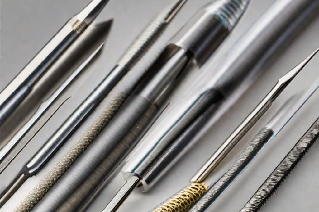
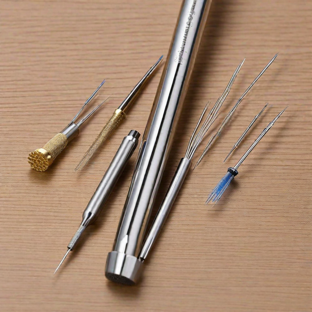
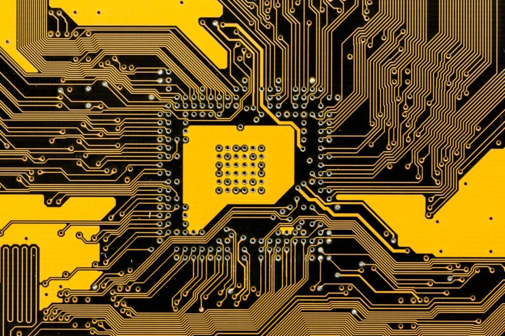
The chemical etching process for titanium creates precision components by selectively removing metal through a photoresist mask. This advanced technique offers numerous advantages over conventional sheet metalworking, including the ability to produce parts without degrading material properties, as no force or heat is used during processing. It also allows for almost limitless part complexity, with component features machined simultaneously using etchant chemistries.
Table of Contents
What is Chemical Etching Titanium and How Does It Work?
Chemical etching titanium is a metalworking process that utilizes specialized corrosive chemicals to etch complex and precise components from titanium. This process is highly favored in modern metal machining due to its high precision, low failure rate, and the unique properties of titanium, such as its high strength-to-weight ratio, corrosion resistance, and biocompatibility.

The chemical etching process for titanium begins by laminating the metal with a light-sensitive photoresist, which is then exposed to UV light to transfer the CAD image of the component. The unexposed photoresist areas are developed and removed, and the exposed metal is sprayed with specific etchant chemicals tailored for titanium to accurately remove the unprotected areas. Finally, the remaining photoresist is stripped away to reveal the finished etched component.
Digital Tooling and Economic Efficiency
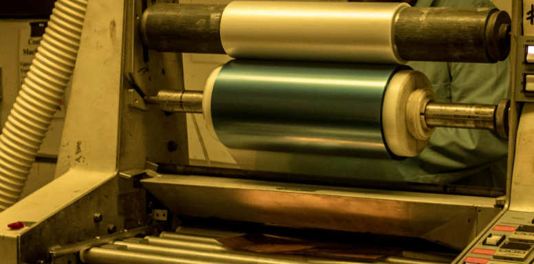
One of the key advantages of chemical etching titanium is its use of digital tooling. Unlike traditional methods that require expensive and difficult-to-adapt steel molds, digital tooling for etching is quick to adapt and change, often within an hour. This ensures that large quantities of products can be reproduced with zero tool wear, guaranteeing that the first and millionth part produced are exactly the same.
The adaptability of digital tooling makes it ideally suited for both prototype and high-volume production runs. This “risk-free” design optimization incurs no financial penalties and boasts a turnaround time that is estimated to be 90% quicker than for stamped parts, which also require substantial upfront investment in mold fabrication.
View our Chemical Etching Titanium process capabilities and pricing packages
[custom_pricing]
Applications of Etched Titanium Components
The chemical etching process is suitable for virtually any titanium component between 0.01mm and 1.5mm in thickness. Here are some examples where chemical etching titanium truly adds value:
-
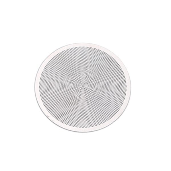
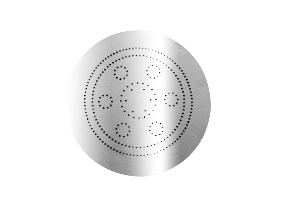
Etching of Ultra-Thin, Ultra-Dense Grating Metal Disk for Optical Applications
Precision etching of a metal disk featuring ultra-thin and ultra-dense grating, designed for optical applications. View our etching production facility WET – Precision Etching Specialist
-
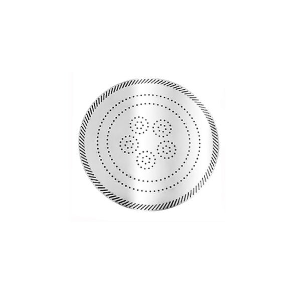
Super Hard Stainless Steel Metal Shim Etching
Accurate etching of super-hard stainless steel metal shims for applications requiring exceptional hardness and durability. View our etching production facility WET – Precision Etching Specialist
Medical Devices and Implants: Titanium is renowned for its biocompatibility and strength, making it ideal for medical implants and devices. Chemical etching allows for the creation of complex and precise components needed in surgical instruments, orthopedic implants, and dental devices, ensuring both functionality and safety.
Aerospace and Defense: Titanium’s high strength-to-weight ratio and corrosion resistance make it indispensable in the aerospace and defense industries. Chemical etching enables the production of intricate components such as lightweight structural parts, heat shields, and detailed engine components, all of which require precision and durability.
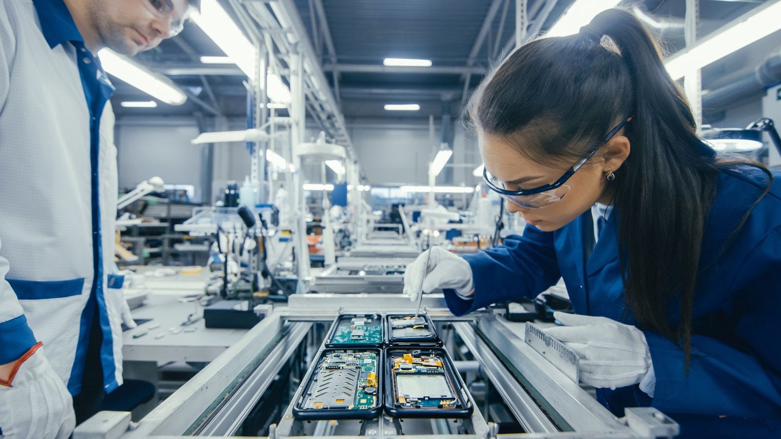
Consumer Electronics: In the consumer electronics sector, titanium is valued for its strength, lightweight nature, and aesthetic appeal. Chemical etching is used to manufacture detailed and complex components for devices such as smartphones, laptops, and wearable technology, ensuring high performance and sleek design.
Automotive Components: The automotive industry benefits from titanium’s properties in applications requiring high strength and corrosion resistance. Chemical etching produces precise parts such as engine components, exhaust systems, and high-performance fasteners, enhancing vehicle performance and longevity.
Summary
Titanium exhibits a range of characteristics that make it ideal for numerous industrial applications. The chemical etching process offers significant advantages for producing complex and safety-critical titanium components, including:
- No expensive hard tooling
- Rapid transition from prototype to production
- Almost unlimited part complexity
- Burr- and stress-free component features
- Unaffected metal properties
- Suitability for all grades, with accuracy to ±0.025 mm
- Lead times measured in days, not weeks or months
The versatility of chemical etching titanium, combined with WET Etched’s extensive experience, makes it a compelling option for manufacturing titanium components across diverse and demanding applications. This process stimulates innovation, removing obstacles inherent in traditional sheet metalworking technologies.