
photo-etching:
– parts without burrs, strains, flashes, or work-hardening.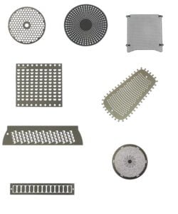
WETETCH produces industrial precise components and other products by photo-etching. In addition to metal etching, we provide everything from “precision etching” with our unique technology to etching on special materials and 3D shapes. We also offer one-stop services for combined processing and surface treatment after etching.
The advantages of photo-etching include:
– Manufacture of perfect precision parts without burrs, strains, flashes, or work-hardening.
– Drastic reduction of initial cost as no expensive tooling is required, unlike stamping work.
– Ideal for prototypes as shorter production and delivery times are possible.
– Suitable for mass production as many pieces can be processed simultaneously.
Introduction to photo-etching
- Metal etching (SUS, Cu, Fe, Ni, etc.)
- Precision hybrid etching (Etching of patented material + electroforming)
- Special metal etching (Mo, Ti, Al, etc.)
- 3D etching (Etching of three-dimensional and curved surfaces)
- Thin-film etching (chemical etching and patterning by depositing metal thin films on various base materials).
1. Metal etching
1. Thickness and size
Processed plate thickness: t = 0.01 mm ~ 0.5 mm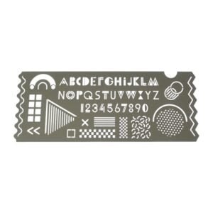
Please contact us for other thicknesses.
Maximum size: 600 x 1100
2. Processing materials
Metals: Stainless steel (SUS304/SUS316/SUS420/SUS430, etc), copper (Cu), iron (Fe), nickel (Ni), nichrome (NCH), and others
3. Working limit
Processing limits vary depending on the thickness of the materials. The following is a general approximation.
The minimum width of D is equivalent to the material thickness, i.e., 0.05 mm, while the minimum size of W is equivalent to half of the material thickness, i.e., 0.03 mm.
t ≦ hole width (which is generally 1.5x bigger than material thickness).
The minimum width of D for mass production is around 0.07 mm.
t ≧ remaining width (Minimum remaining width is 70% of material thickness)
| Material thickness(t) | Minimum hole width (D) | Minimum remaining width |
|---|---|---|
| t ≦ 0.05 | To be determined by a test run | To be decided by test run |
| Over t=0.05 | t×100% | About t×70% |
4. Dimensional tolerance
Although tolerance changes depending on thickness and shape, ±10-15% of thickness is standard tolerance. For other details, please contact us.
5. Side edges
Due to the nature of photo etching, it is unavoidable that the cross-section of the etched edge is not completely vertical. The length of this side edge is within 10%-20% of the plate thickness. We consider the material, shape, and thickness of the product and use precisely managed correction techniques to manufacture the most optimal product.
6. Double-side and single-side etching
Double-side etching: Both the front and the back sides of the material are corroded and melted by an etching solution to penetrate the material, which is the general method.
Single-side etching: Only one side of the material is corroded and melted to make a hole in the material.
7. Half-etching
Different from full (penetrating) processing, this technique engraves a pocket shape to a depth of around half of the material’s thickness. Combining half-etching with full (penetrating) etching allows us to produce intricate designs.
8. Tab properties
In the etching process, tabs are required to connect the product with the frame. If you have any preferences for the position and shape of the tabs, please contact us in advance. We also provide a non-tabbed product.x
Etching special materials(Mo/Ti/Al/etc.)
Special materials that are hard-to-cut such as molybdenum, titanium, and aluminum can be etched at our factory. Please contact us about Elgiloy/Inconel/Hastelloy and other special materials.

| thickness(t) | 0.01 | 0.02 | 0.05 | 0.10 | 0.15 | 0.30 |
|---|---|---|---|---|---|---|
| tolerance | ±0.004 | ±0.007 | ±0.010 | ±0.015 | ±0.020 | ±0.030 |
Thin-film etching
The thin-film metal which is vapor-deposited on various base materials is chemically etched to make patterns. Etching on thin film material that is sputtered and vaporized such as ITO, Aluminum, Zinc Sulfide, and Nickel is carried out to create intricate patterns.
Technology highlights
- A variety of base materials can be processed, from plastic such as polycarbonate, PET, and acrylic, to glass and metals.
- Thin-film metal: Ai, Ni, Cu, Cr, Zn, Ti, Si, Nb, Mo, W, S, etc.
- Base material: glass, ceramic, glass epoxy, PI, PC, PMMA, PET, metal, etc.
- Base material exterior processing: Material exteriors can be stamped and cut all while maintaining the positional accuracy of the patterns.