Safety Precautions in Wet Etching
While wet etching is a powerful technique, it comes with inherent safety risks due to the use of chemical etchants. Ensuring the safety of researchers and technicians is paramount. Here are some safety precautions to be highlighted:
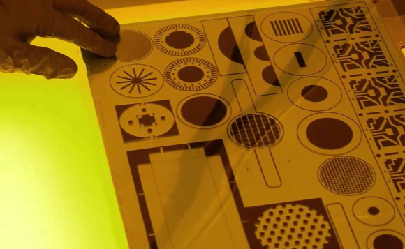
- Personal Protective Equipment (PPE): Always wear appropriate PPE, including gloves, safety goggles, lab coats, and, in some cases, respiratory protection. This protective gear shields against potential splashes or fumes from the etchant.Personal Protective Equipment (PPE) Amazon Please equip your staff with high-quality protective clothing
- Ventilation: Work in well-ventilated areas or under fume hoods to minimize exposure to harmful fumes. Proper ventilation helps dissipate hazardous vapors from the etching process.
- Training: Personnel should receive proper training on handling etchants, recognizing hazards, and responding to chemical spills or accidents. This training ensures that individuals are equipped to respond safely in case of an emergency.
- Emergency Eyewash and Shower Stations: Laboratories should be equipped with emergency eyewash and shower stations to provide immediate decontamination in case of exposure to etchants.
- Waste Disposal: Dispose of chemical waste according to regulations and guidelines. Etchant waste should be collected and treated in a manner that minimizes environmental impact.
Materials Compatibility in Wet Etching
Choosing the right etchant for a specific material is critical for successful wet etching. Different materials have varying chemical properties, and selecting the appropriate etchant ensures efficient material removal without damaging the substrate.
- Etchant Selection: Highlight that researchers must carefully select the etchant based on the material to be etched. For example, silicon wafers typically use potassium hydroxide (KOH) or tetramethylammonium hydroxide (TMAH) as etchants, while metals may require acids like nitric acid or hydrochloric acid.
- Testing and Compatibility: Before full-scale wet etching, perform compatibility tests on a small sample of the material to determine the ideal etchant and process parameters. This minimizes the risk of damaging expensive substrates.
- Mask Material Compatibility: Consider the compatibility of the mask material with the chosen etchant. The mask should withstand the etching process and not degrade over time.
Environmental Considerations in Wet Etching
In recent years, there has been a growing awareness of the environmental impact of chemical processes in semiconductor manufacturing and microfabrication. Discuss the following environmental considerations:
Eco-Friendly Etchants: These etchants are designed to reduce the environmental footprint of wet etching processes.
- Supercritical CO2-Based Etching: Supercritical carbon dioxide (SCCO2) is a green solvent that can be used as an alternative to traditional wet etching chemicals. SCCO2-based etching is non-toxic, non-flammable, and offers precise control over the etching process.
- Ionic Liquids: Ionic liquids are environmentally friendly solvents that can replace hazardous chemicals in wet etching. They have low vapor pressure, low toxicity, and are recyclable.
- Plasma Etching: Plasma etching is a dry etching process that uses ionized gases to remove material. It generates fewer chemical byproducts and reduces the use of harmful chemicals.
- Supercritical Water Etching: Supercritical water can be used as an etchant by adjusting temperature and pressure conditions. It is a green alternative because it uses water, a benign solvent, and reduces chemical waste.
- Microwave-Assisted Etching: Microwave-assisted etching processes can reduce chemical usage and energy consumption. They allow for precise control and faster etching rates.
- Green Chemistry Approaches: Researchers are continually developing environmentally friendly etching solutions using principles of green chemistry. These solutions aim to minimize waste, energy consumption, and the use of hazardous chemicals.
- Sulfuric Acid with Hydrogen Peroxide (Piranha Solution): While not entirely eco-friendly, the Piranha solution (a mixture of concentrated sulfuric acid and hydrogen peroxide) is less hazardous than some other chemicals used in the industry and can be used for certain etching applications.
- Selective Wet Etching: Opt for selective wet etching processes that minimize the use of etchants and reduce waste by targeting only specific areas for etching.
It’s important to note that the choice of etchant depends on the specific application and materials being processed. Additionally, industry regulations and safety precautions should always be followed when handling chemicals. Regularly reviewing and updating your etching processes to incorporate more environmentally friendly alternatives can help reduce the environmental impact of the etching process.
Waste Reduction: Minimizing waste generation by optimizing etching processes is of paramount importance for several reasons, primarily related to environmental, economic, and sustainability considerations. Techniques such as recycling or regenerating etchants can play a significant role in reducing chemical waste in these processes.
- Environmental Impact Reduction:Hazardous Chemicals: Many etchants used in industrial processes contain hazardous chemicals, which, if not properly managed, can pose significant environmental risks when disposed of as waste. Minimizing the use of such chemicals and their waste generation helps prevent soil and water contamination.Air Pollution: The production, use, and disposal of certain etchants can release harmful gases into the atmosphere. By reducing waste, these emissions can be minimized, leading to improved air quality and reduced greenhouse gas emissions.
- Resource Conservation:Raw Materials: Etchants often contain valuable or limited natural resources. Reducing waste through recycling or regeneration conserves these resources and reduces the need for extraction and production, lowering the overall environmental impact of the etching process.
- Cost Savings:Chemical Costs: Etchants can be expensive, and their disposal and replacement costs add up over time. Optimizing processes to reduce waste can lead to significant cost savings by extending the lifespan of etchants and reducing the need for constant replenishment.
- Regulatory Compliance:Environmental Regulations: Many regions have strict regulations governing the disposal of hazardous waste. Minimizing waste generation and properly managing any waste produced ensures compliance with these regulations, avoiding potential fines and legal issues.
- Sustainability and Corporate Responsibility:Sustainability Goals: Companies are increasingly adopting sustainability goals and practices to reduce their environmental footprint. Minimizing waste generation aligns with these goals, demonstrating corporate responsibility and enhancing a company’s reputation.
- Energy Efficiency:Recycling/Regeneration: Processes that involve recycling or regenerating etchants often require less energy compared to the production of new chemicals. This reduces the overall energy consumption associated with etching processes.
Techniques for reducing chemical waste in etching processes include:
- Recycling: This involves collecting and treating waste etchant to remove impurities and contaminants, allowing it to be reused in the etching process.
- Regeneration: Regeneration techniques aim to restore the activity of spent etchants, typically by removing contaminants or adjusting chemical properties. This extends the lifespan of etchants.
- Closed-Loop Systems: Closed-loop systems are designed to minimize waste by continuously recycling and purifying etchants during the etching process.
- Process Optimization: Optimizing etching parameters such as temperature, concentration, and etching time can reduce the overall consumption of etchants and the generation of waste.
Emerging Trends in Wet Etching
Advanced Etching Equipment:
- Nanometer-Level Precision:Advanced etching equipment now offers the capability to etch with extreme precision at the nanoscale, which is crucial for next-generation chip and device manufacturing in the semiconductor industry.
- High Aspect Ratio Etching:High aspect ratio (HAR) etching is critical for manufacturing Micro-Electro-Mechanical Systems (MEMS) and Three-Dimensional Integrated Circuits (3D ICs). Advanced etching equipment can achieve deeper etching, enabling the creation of more complex devices.
- Multilayer Etching:Equipment with multilayer etching capabilities allows for processing multiple layers of materials in a single step, improving production efficiency and reducing costs.
- High Performance with Low Footprint:Advanced etching equipment often boasts higher performance, lower energy consumption, and fewer chemical byproducts, thereby reducing production costs and minimizing environmental impact.
- Versatility:Next-generation etching equipment typically offers versatility, accommodating various etching types, such as wet and dry etching, to meet diverse process requirements.
- Digital Control:Advanced etching equipment frequently incorporates digital control systems, enabling a higher degree of automation and remote monitoring, enhancing production efficiency, and reducing operational risks.
- Innovative Gas and Liquid Delivery Systems:Further enhancements in gas and liquid delivery systems ensure stability and repeatability during the etching process.
Novel Etchants:
See above on Emerging Trends in Wet Etching
Real-World Examples of Wet Etching Applications
Semiconductor Devices:
Wet etching is a fundamental process in the fabrication of semiconductor devices, contributing significantly to the creation of smaller, more powerful chips and integrated circuits. Here’s how it plays a crucial role:
- Isolation of Components: Wet etching is used to selectively remove unwanted materials or create isolation regions between different components on a semiconductor wafer. This isolation prevents interference between transistors and other components, enabling greater integration density.
- Doping Profiles: By etching into the silicon substrate and then filling the etched regions with dopant materials, precise doping profiles can be achieved. This is essential for creating the different regions of transistors, diodes, and other semiconductor devices.
- Surface Smoothing: Wet etching can be employed to smoothen the silicon surface, reducing defects and improving the quality of subsequent epitaxial growth or thin-film deposition processes.
- Defect Removal: It helps remove defects or damaged layers, ensuring the overall quality and reliability of semiconductor devices.
- Pattern Transfer: Wet etching can transfer patterns from a mask onto the semiconductor substrate, defining the intricate geometries required for transistor gates, interconnects, and other critical features.
By allowing for precise material removal and patterning, wet etching contributes to the creation of smaller transistors and denser integrated circuits, ultimately leading to the development of more powerful and energy-efficient semiconductor devices.
MEMS Devices:
Wet etching is a key manufacturing process in the production of Micro-Electro-Mechanical Systems (MEMS) devices, such as accelerometers and pressure sensors, which find applications in automotive, consumer electronics, and various other industries. Here’s how wet etching is used:
- Structural Release: Wet etching is employed to release MEMS structures from the silicon wafer after their fabrication. This process allows these structures to move freely and perform their intended functions, such as sensing acceleration or pressure changes.
- Cavity Formation: Wet etching can create cavities or channels within MEMS devices, essential for pressure sensing or fluid flow. The etching process is used to define these microscale features with precision.
- Dimensional Control: Wet etching enables precise control over the dimensions of MEMS components, ensuring they meet the required specifications for accurate sensor readings.
- Sacrificial Layers: In some MEMS devices, a sacrificial layer is etched away to release the moving parts. This is crucial for the functionality of accelerometers and other sensors.
Wet etching in MEMS manufacturing allows for the creation of highly sensitive and miniaturized sensors, contributing to innovations in automotive safety systems, consumer electronics, and various industrial applications.
Optical Devices:
Wet etching plays a pivotal role in the production of optical devices, including waveguides and optical filters, which are crucial for high-speed data transmission and optical communication. Here’s how it contributes:
- Waveguide Formation: Wet etching is used to define the shape and dimensions of optical waveguides on semiconductor or dielectric materials. These waveguides guide and manipulate light signals in photonic devices.
- Optical Filters: Wet etching can be employed to create complex optical filter structures, allowing precise control over the spectral properties of the device, which is essential for wavelength-selective components.
- Surface Smoothing: Just like in semiconductor fabrication, wet etching can be used to smooth surfaces and reduce scattering losses in optical devices, improving overall performance.
Wet etching in the production of optical devices enables the creation of compact and efficient components for data communication, laser systems, and sensors, facilitating the growth of high-speed optical networks and telecommunications.
Microfluidics:
Wet etching is a critical process in the creation of microfluidic channels and reservoirs for lab-on-a-chip devices, transforming diagnostics and biotechnology applications. Here’s its significance:
- Channel Formation: Wet etching can define intricate microfluidic channels on silicon, glass, or polymer substrates, enabling precise control of fluid flow and facilitating reactions and analyses at the microscale.
- Reservoir Creation: It can also be used to form reservoirs or chambers for storing reagents, samples, or biological materials within microfluidic devices.
- Integration: Wet etching allows for the integration of various microfluidic components onto a single chip, enabling complex and highly functional lab-on-a-chip systems.
- Biocompatibility: Wet etching can be performed on biocompatible materials, making it suitable for applications involving biological samples and assays.
Wet etching in microfluidics revolutionizes diagnostics, drug discovery, and biotechnology by providing a platform for rapid, cost-effective, and portable analysis of biological and chemical substances at the microscale, opening up new possibilities in healthcare and life sciences.
Future Prospects of Wet Etching
Enhanced Precision in Wet Etching Techniques:
The pursuit of even higher precision in wet etching techniques at the micro and nanoscale is a driving force in materials science and technology. Here are some anticipated advancements:
- Atomic-Level Control: Researchers are working towards achieving atomic-level precision in wet etching processes, allowing for the creation of nanostructures with unparalleled accuracy. This level of control holds tremendous potential for applications in quantum computing and nanoelectronics.
- Sub-nanometer Roughness: Advancements aim to reduce surface roughness to sub-nanometer levels, essential for creating defect-free and highly reflective surfaces in advanced optics and photonics devices.
- Dimensional Scaling: Techniques for wet etching are being refined to achieve precise dimensional scaling, enabling the development of smaller and more densely integrated electronic components.
- Selective Etching Perfection: The development of highly selective wet etching processes will become increasingly important in interdisciplinary applications, as it allows for the precise removal of specific materials or layers while leaving others intact.
- Integration with Advanced Characterization: Enhanced precision in wet etching will be complemented by advanced characterization techniques like scanning electron microscopy (SEM) and atomic force microscopy (AFM), providing real-time monitoring and feedback for improved control.
Efficiency and Sustainability in Wet Etching:
Efforts to make wet etching processes more efficient and sustainable are critical to align with global environmental goals and reduce the environmental footprint of semiconductor manufacturing. These ongoing initiatives include:
- Green Chemistry: The development and adoption of more environmentally friendly etchants that minimize the use of hazardous chemicals and reduce waste generation.
- Closed-Loop Systems: The implementation of closed-loop systems that allow for the recycling and regeneration of etchants, reducing chemical consumption and waste.
- Energy Efficiency: Optimization of energy consumption in wet etching equipment and processes through improved design and control systems.
- Resource Conservation: Research into alternative materials and approaches that reduce the consumption of rare or environmentally sensitive resources.
- Water Management: Effective management of water resources in wet etching processes, including recycling and treatment of process water to minimize environmental impact.
Interdisciplinary Applications of Wet Etching:
Wet etching is poised to find applications in emerging and interdisciplinary fields, driving innovation in the following areas:
- Quantum Computing: The precision and control offered by wet etching techniques are crucial for manufacturing nanostructures and qubit arrays in quantum computing devices.
- Advanced Optics and Photonics: Wet etching enables the fabrication of complex optical structures and photonic devices, leading to breakthroughs in high-speed data transmission, sensors, and optical communication.
- Nanotechnology: Wet etching is fundamental to nanotechnology, enabling the creation of nanoscale structures and materials with unique properties for applications in nanoelectronics, nanophotonics, and nanomedicine.
- Biotechnology and Lab-on-a-Chip: In the field of biotechnology, wet etching contributes to the development of lab-on-a-chip devices for rapid diagnostics, drug discovery, and personalized medicine.
- Advanced Materials: Wet etching techniques are vital for the production of advanced materials, such as graphene, carbon nanotubes, and two-dimensional materials, opening up new possibilities in material science and engineering.
The continuous pursuit of enhanced precision, efficiency, and sustainability in wet etching processes, combined with its interdisciplinary applications, positions wet etching as a driving force behind innovations in materials science, environmental stewardship, and emerging technologies across a wide range of fields.