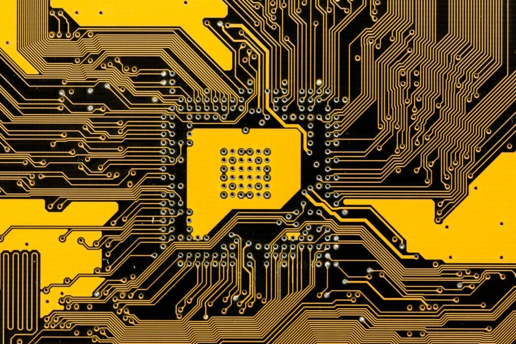
Semiconductor etching is a crucial step in the fabrication of electronic devices, allowing for the precise removal of material layers from semiconductors. This process is instrumental in creating the intricate patterns necessary for the functioning of integrated circuits.
If you want to produce PCBs, or semiconductors independently. Then I will disabuse you of the idea, because trying to produce PCBs or semiconductors complete and independently, I don’t think any company can afford the investment cost.
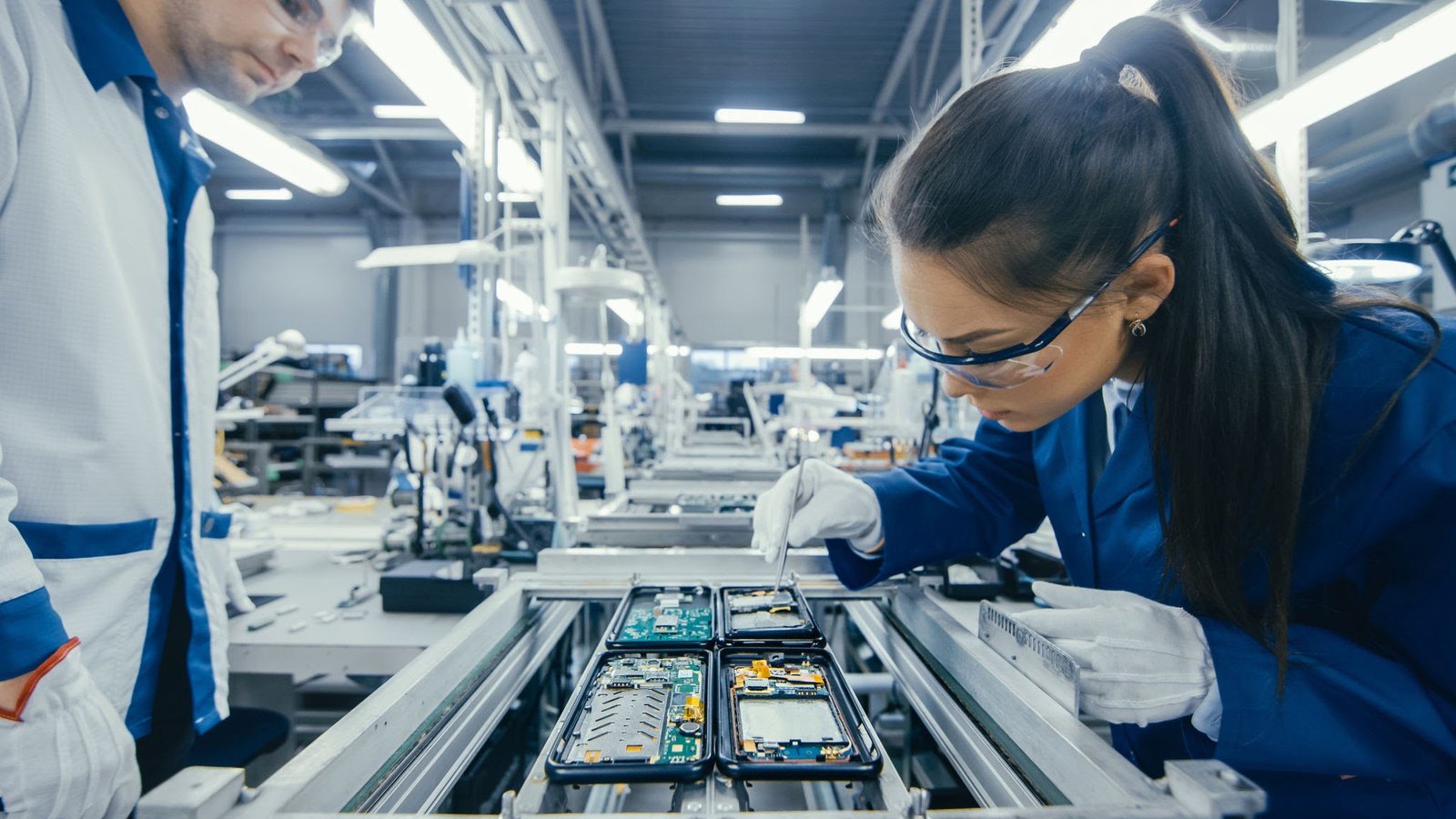
Let’s start simply by understanding the PCB fabrication process.
1. Semiconductor Etching Equipment:
1.1 LDI High-Precision Exposure Machine: The LDI (Laser Direct Imaging) high-precision exposure machine plays a vital role in the semiconductor etching process. This equipment uses laser technology to selectively expose photoresist-coated semiconductor wafers, defining the patterns that will guide the subsequent etching steps. LDI machines offer exceptional precision, enabling the production of intricate and miniaturized semiconductor components.
1.2 Chemical Etching Equipment: Chemical etching equipment is designed to selectively remove material layers from semiconductor wafers. Among the common types are wet chemical etching and dry etching systems.
- Wet Chemical Etching:
- Equipment Overview: Wet chemical etching involves immersing the semiconductor wafer in a chemical solution to selectively remove material.
- Role: The equipment facilitates controlled material removal, allowing for the creation of precise patterns.
- Common Equipment: Manufacturers such as Dragon Etching provide wet chemical etching systems, ensuring uniform and controlled etching processes.
- Dry Etching Systems:
- Equipment Overview: Dry etching, including techniques like reactive ion etching (RIE) and plasma etching, employs gases and plasmas to remove material.
- Role: These systems offer high-precision etching with minimal damage to the underlying material.
- Common Equipment: Oxford Instruments is a reputable manufacturer of dry etching systems, providing solutions for various semiconductor materials.
2. Common Etchants in Semiconductor Etching:
Analyzing several common etchants is crucial to understanding their application and parameters. Below is a table summarizing some commonly used etchants:
| Etchant | Composition | Selectivity | Temperature (°C) | Etch Rate (nm/min) |
|---|---|---|---|---|
| Buffered HF | HF + NH4F | High | Ambient | ~1 – 10 |
| Piranha Solution | H2SO4 + H2O2 | Moderate | Ambient | Variable |
| KOH | KOH | High | ~50 – 80 | ~50 – 100 |
| SF6 Plasma | SF6 + O2 | High | ~50 – 100 | ~10 – 100 |
3. Basic Applications of Semiconductor Etching:
The semiconductor etching process finds applications in various industries, including:
- Glass Etching: Used for creating microstructures on glass surfaces.

- Silicon Wafer Etching: Critical in the production of integrated circuits.

- MEMS (Micro-Electro-Mechanical Systems): Enables the fabrication of miniature mechanical components on semiconductor wafers.
Semiconductor Etching Process Flow:
3.1. Photoresist Application:
- A thin layer of photoresist is applied to the semiconductor wafer.
3.2. Exposure:
- The LDI high-precision exposure machine selectively exposes the photoresist to define the desired patterns.
3.3. Development:
- The exposed photoresist is developed, revealing the pattern on the semiconductor surface.
3.4. Etching:
- The semiconductor wafer undergoes wet or dry etching, selectively removing material based on the developed pattern.
3.5. Resist Stripping:
- Any remaining photoresist is removed, leaving behind the etched semiconductor pattern.
Semiconductor etching is a sophisticated process with a range of specialized equipment and etchants, crucial for the production of advanced electronic devices. Understanding the intricacies of this process is essential for achieving precision and efficiency in semiconductor fabrication.
If you have PCB or semiconductor processing in mind, please do not hesitate to contact us. Contact us today. We will provide you with processing and manufacturing services. All you need to do is provide us with the appropriate drawings.

Frequently Asked Questions
What is Understanding Semiconductor Etching and how is it made?
Understanding Semiconductor Etching is produced by photochemical etching — a process that uses a patterned resist and etchant to remove metal precisely, with no mechanical stress or burrs.
What tolerances can you achieve for Understanding Semiconductor Etching?
Photochemical etching holds tight, repeatable tolerances on thin metal, which makes it well suited to Understanding Semiconductor Etching. Exact figures depend on material and thickness.
Can Understanding Semiconductor Etching be customised to my drawing?
Yes. Understanding Semiconductor Etching is made to order from your CAD/artwork, so dimensions, features and material are all tailored to your specification.
What is the typical lead time and minimum order for Understanding Semiconductor Etching?
Because etching needs no hard tooling, Understanding Semiconductor Etching can be prototyped quickly and scaled to volume. Share your drawing and quantity and we will advise lead time.