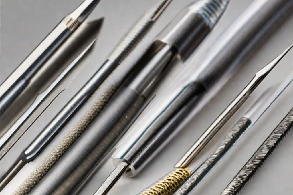
WET is a professional manufacturer of high-quality tungsten probes for batch customization. In the realm of precision engineering, where every micron matters, fine tungsten probes emerge as indispensable tools driving innovation and discovery. As manufacturers strive to meet the exacting demands of various industries, the role of fine tungsten probe batch customization becomes paramount.

| Parameter | Description | Typical Range | Application Areas |
|---|---|---|---|
| Probe Tip Diameter | Diameter of the probe tip | 0.001 – 0.020 inches | Precision Instrument Probes, Microelectronics |
| Tip Radius | Radius of the probe tip | 0.0005 – 0.005 inches | Semiconductor Testing, Nanotechnology |
| Taper Length | Length of the taper portion | 0.010 – 0.200 inches | Biomedical Research, DNA Sequencing |
| Overall Length | Total length of the tungsten probe | 0.050 – 1.000 inches | Electronics Testing, Material Analysis |
| Shaft Diameter | Diameter of the probe shaft | 0.005 – 0.050 inches | MEMS (Microelectromechanical Systems) |
| Coating | Optional coating for enhanced properties | Various options available | Optoelectronics, Optical Fiber Testing |
Detailed Application Areas:
- Precision Instrument Probes: Tungsten probes with precise tip diameters and tip radii are commonly used for probing and testing delicate instruments and components in precision engineering applications.
- Microelectronics: Tungsten probes find extensive use in the microelectronics industry for testing integrated circuits, probing microchips, and analyzing semiconductor materials.
- Semiconductor Testing: Tungsten probes with sharp tip radii are essential for semiconductor testing, where they enable precise probing of small features on silicon wafers and other semiconductor substrates.
- Nanotechnology: Tungsten probes with ultrafine tip radii are indispensable tools in nanotechnology research, enabling scientists to manipulate and characterize nanoscale structures with unparalleled precision.
- Biomedical Research: Tungsten probes with specialized coatings and precise tip geometries are utilized in biomedical research for applications such as cellular probing, electrophysiology, and neurostimulation.
- DNA Sequencing: Tungsten probes are employed in DNA sequencing applications, where they facilitate the manipulation and analysis of DNA molecules with high precision and accuracy.
- Electronics Testing: Tungsten probes are used in various electronics testing applications, including printed circuit board (PCB) testing, device characterization, and failure analysis.
- Material Analysis: Tungsten probes are utilized in material analysis applications such as scanning electron microscopy (SEM), atomic force microscopy (AFM), and surface profilometry for precise surface characterization and analysis.
- MEMS (Microelectromechanical Systems): Tungsten probes play a crucial role in MEMS fabrication and testing, where they enable precise probing and manipulation of microscale structures and devices.
- Optoelectronics: Tungsten probes are used in optoelectronics applications for testing and characterizing optical components, photonic devices, and fiber-optic systems.
If you have Custom tungsten needles, please feel free to contact us.
FAQs
What metals can you use to customize my goods?
- Wet Etching Germanium
- Wet Etching Gallium Nitride (GaN)
- Wet Etching Indium
- Wet Etching Cobalt
- Wet Etching Tungsten
- Wet Etching Stainless Steel
- Wet Etching Aluminum
- Wet Etching Kovar
- Wet Etching Copper
- Wet Etching Steel
- Wet Etching Nickel
- Wet Etching Platinum
- Wet Etching Silver
- Wet Etching Rhodium
- Wet Etching Hafnium
- Wet Etching Vanadium
- Wet Etching Zirconium
- Wet Etching Titanium
- Wet Etching Niobium
- Wet Etching Tantalum
- Wet Etching Molybdenum
- Wet Etching Brass
- Wet Etching Rhenium
How quickly can I get your response?
Within 24 hours.
Will you do 100% inspection before shipping out the orders?
Yes we do.
Can I have prototypes or samples before placing the order?
Samples are always available.
Crafting Precision: The Art of Fine Tungsten Probe Manufacturing
Crafting fine tungsten probes is a symphony of precision and expertise. Beginning with meticulously sourced tungsten materials, manufacturers employ advanced manufacturing techniques to transform raw materials into intricate probes. Through a series of refining processes, including precision grinding, shaping, and polishing, each probe is meticulously crafted to meet the highest standards of accuracy and durability.
Tailored to Perfection: The Importance of Batch Customization
In today’s fast-paced industries, where unique applications demand tailored solutions, batch customization emerges as a game-changer. Manufacturers of fine tungsten probes recognize the diverse needs of their clientele and offer bespoke solutions to meet specific requirements. Whether it’s adjusting the tip radius, length, or shape of the probe, customization ensures that each batch of probes is perfectly suited to its intended application.
Precision Meets Performance: Applications of Customized Tungsten Probes
The applications of customized tungsten probes span a myriad of industries, from semiconductor manufacturing and electronics testing to biomedical research and beyond. In the semiconductor industry, customized probes play a crucial role in probing and testing integrated circuits with unparalleled precision. In biomedical research, they enable scientists to explore the intricate world of cellular biology and nanotechnology, driving breakthrough discoveries and innovations.
The Future of Precision Engineering: Innovations in Tungsten Probe Customization
As technology advances and industries evolve, the future of precision engineering holds boundless possibilities. Innovations in materials science, manufacturing techniques, and customization capabilities promise to elevate the performance and versatility of tungsten probes to new heights. From nano-scale probing to space exploration, customized tungsten probes are poised to redefine the boundaries of precision engineering and shape the future of innovation.
Partnering for Precision: Choosing the Right Manufacturer
In the quest for precision, choosing the right manufacturer is paramount. When selecting a partner for fine tungsten probe customization, look for a company with a proven track record of expertise, reliability, and customer satisfaction. By partnering with a trusted manufacturer, you can unlock the full potential of customized tungsten probes and propel your projects to new levels of accuracy and performance.
Frequently Asked Questions
What tolerances can you achieve for Fine tungsten probe batch customization manufacturer?
Photochemical etching holds tight, repeatable tolerances on thin metal, which makes it well suited to Fine tungsten probe batch customization manufacturer. Exact figures depend on material and thickness.
Can Fine tungsten probe batch customization manufacturer be customised to my drawing?
Yes. Fine tungsten probe batch customization manufacturer is made to order from your CAD/artwork, so dimensions, features and material are all tailored to your specification.
What is the typical lead time and minimum order for Fine tungsten probe batch customization manufacturer?
Because etching needs no hard tooling, Fine tungsten probe batch customization manufacturer can be prototyped quickly and scaled to volume. Share your drawing and quantity and we will advise lead time.
Which industries use Fine tungsten probe batch customization manufacturer?
Fine tungsten probe batch customization manufacturer is used across electronics, medical, automotive, aerospace and industrial filtration — anywhere precise, burr-free thin-metal parts are required.