Kovar Etching Process Demonstration
For decades, engineers have grappled with the “expansion mismatch” problem—where a chip heats up, expands, and eventually cracks its seal because the carrier expands at a different rate. The solution lies in Kovar alloy, a nickel-cobalt ferrous alloy designed to match the Coefficient of Thermal Expansion (CTE) of borosilicate glass and alumina ceramics.
However, the material is only half the battle. How you shape that material determines whether the hermetic seal will hold or fail under pressure.
What are Chemical Etched Robust Chip Carriers?
A robust chip carrier is the physical “envelope” that protects integrated circuits from moisture, ionic contaminants, and atmospheric gases. When we specify “chemically etched” carriers, we are referring to components manufactured through Photochemical Machining (PCM).
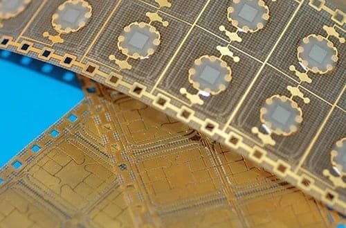
In this process, Kovar sheets are coated with a light-sensitive photoresist, exposed to UV light through a high-resolution tool, and then sprayed with chemical etchants. This removes the unwanted metal atom-by-atom, leaving behind a complex, burr-free part. Because the process is chemical rather than mechanical, it maintains the hermetic integrity required for long-term reliability in harsh environments.
Why Do We Need Chemical Etching?
You might wonder: why not just stamp or laser-cut these parts? The answer lies in the molecular stability of the Kovar itself.
- Stress-Free Fabrication: Unlike stamping, which exerts tons of pressure and induces internal mechanical stress, chemical etching is a “cold” process. It does not alter the grain structure of the Kovar, ensuring the CTE remains uniform across the entire part.
- No Heat-Affected Zones (HAZ): Laser cutting generates intense heat at the edges. For Kovar, this local heating can slightly alter the alloy’s properties, potentially leading to micro-cracks during the glass-to-metal sealing process. Etching eliminates this risk.
- Complex Geometry at No Extra Cost: Etching allows for intricate lead frames and internal features that would be impossible or prohibitively expensive to achieve with traditional tooling.
Process Comparison: Chemical Etching vs. Alternative Methods
When choosing a manufacturing route, it’s vital to see how photochemical machining stacks up against more common industrial techniques:
| Feature | Chemical Etching | Laser Cutting | Stamping |
| Edge Quality | Burr-free & Smooth | Slag/Dross presence | Shear/Break edges |
| Material Stress | Zero | Thermal Stress | Mechanical Stress |
| Tooling Cost | Low (Digital Film) | Zero | High (Hard Die) |
| Lead Time | Days | Hours/Days | Weeks/Months |
| Precision | Ultra-High | High | Moderate |
Technical Specifications and Data
To ensure a perfect hermetic seal, precision is the primary metric. Chemical etching excels in thin-gauge Kovar applications where tight tolerances are non-negotiable.
- Thickness Range: $0.05\text{ mm}$ to $0.3\text{ mm}$ (Standard for most high-density carriers).
- Dimensional Tolerance: $\pm 0.01\text{ mm}$ (Ensuring perfect alignment with ceramic bases and glass preforms).
- Surface Finish: Maintained at the original mill specification, ideal for subsequent gold or nickel plating.
Critical Applications: Where Precision Meets Survival
Chemical Etching Kovar carriers are not found in your everyday smartphone; they are reserved for environments where “failure” isn’t an option.
1. Aerospace and Defense
In satellite communication systems, components face extreme temperature swings. Kovar carriers are integrated into Transmit/Receive (T/R) Modules and Microwave Hybrid Circuits found in phased-array radars. The CTE matching ensures that as the satellite moves from the sun’s heat to the earth’s shadow, the vacuum seal remains intact.
2. Medical Implantable Devices
Devices like Pacemakers and Cochlear Implants utilize etched Kovar frames within their hermetic enclosures. The smooth, burr-free edges provided by etching prevent any sharp points from puncturing delicate internal membranes or causing interference with bio-sensors.
3. High-End Optical Equipment
You will find these robust carriers inside Infrared (IR) Imaging Sensors and Laser Diode Packages. Because these devices are often cryogenically cooled, the stress-free nature of the etched Kovar prevents the “optical tilt” that occurs when stressed metals warp at low temperatures.
Chemical etching machine