Chrome/Quartz Photomask Fabrication Animation
In the microfabrication industry, the photomask (or photolithography mask) is the master template that defines the intricate patterns transferred onto semiconductor wafers, microelectromechanical systems (MEMS), and flat-panel displays. Among the most demanding mask types are those fabricated on chrome-coated quartz substrates, where the chrome layer serves as the opaque pattern-defining material and the quartz provides exceptional optical transparency and thermal stability. According to industry standards, the quality of photomask patterns is directly tied to critical dimension (CD) control, which becomes increasingly stringent with each successive technology node.
While traditional mask-making relies heavily on direct-write laser or electron-beam lithography followed by subtractive etching, the process of chemical etching—specifically wet etching of the chrome layer and dry etching of quartz for phase-shift applications—remains the critical step that determines critical dimension (CD) accuracy, edge roughness, and final pattern fidelity. This article details the step-by-step fabrication process of chrome/quartz photomasks, the specialized equipment involved, and the broad range of industries and end-use equipment that depend on these precision masks.
Photomask Manufacturing & Applications
| Category | Sub-Category | Key Details | Equipment / Tools Used |
|---|---|---|---|
| Base Materials | Substrate | Fused silica (quartz), low thermal expansion | Optical flatness measurement, spectrophotometer |
| Opaque Layer | Chromium (Cr), 50–100 nm thickness | Sputtering system | |
| Anti-reflective Layer | Chromium oxide (CrOₓ) | Sputtering system | |
| Phase-Shift Layer | MoSiON for half-tone masks | PECVD or sputtering | |
| Key Process Steps | Photoresist Coating | Positive-tone, chemically amplified resist (CAR) | Spin coater, hotplate |
| Pattern Writing | Direct-write laser or e-beam | Laser pattern generator, E-beam lithography system | |
| Chrome Etching | Wet etch: CAN/HNO₃; Dry etch: chlorine-based plasma | Spin-etch processor, decoupled plasma etcher | |
| Quartz/MoSi Etching | Dry etch: fluorine-based plasma (CF₄, CHF₃, O₂) | Decoupled plasma etcher with bias control | |
| Metrology | CD measurement, thin film characterization, OCD | CD-SEM, scatterometer, reflectometer | |
| Inspection | Defect detection, pattern verification | Die-to-database inspection system, AOI | |
| Repair | Opaque/clear defect correction | FIB repair tool, gas-assisted deposition system | |
| Applications | Semiconductor | Logic, memory, advanced nodes (7nm and beyond) | DUV/EUV scanners (ASML, Nikon, Canon) |
| Flat Panel Display | TFT-LCD, AMOLED, LTPS, IGZO, LTPO | FPD exposure tools (Nikon, Canon) | |
| MEMS | Accelerometers, gyroscopes, microfluidics | Mask aligners (SÜSS, EVG) | |
| Optoelectronics/LED | LED epitaxial wafers, optoelectronic devices | Maskless lithography tools | |
| Advanced Packaging | RDL, TSV, fan-out wafer-level packaging | Wafer-level packaging steppers | |
| Telecommunications | 5G RF devices, GaN/SiC power electronics | i-line/g-line steppers |
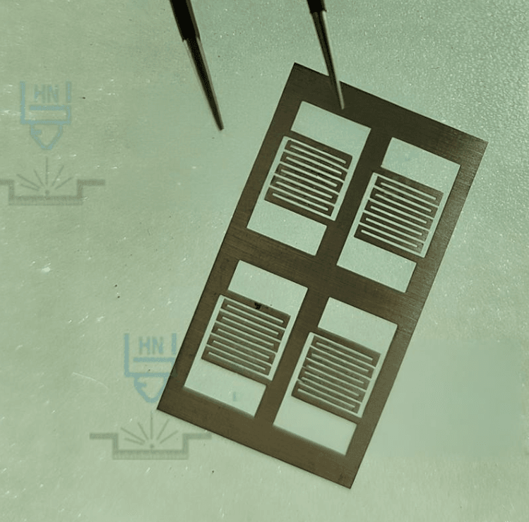
The Fabrication Process of Chrome/Quartz Photomasks
The production of high-accuracy photomasks is a multi-stage process conducted in ultra-clean environments (Class 1 or Class 10 cleanrooms). Each step is designed to preserve the integrity of the quartz substrate and the chrome pattern, ensuring that critical dimensions are maintained within tolerances of tens of nanometers.
Step 1: Substrate Preparation and Incoming Inspection
The process begins with the selection of high-quality fused silica (quartz) blanks, which are preferred for deep ultraviolet (DUV) and vacuum ultraviolet (VUV) applications due to their low thermal expansion and high transmittance down to 193 nm. These blanks are pre-coated with a thin, uniform layer of chromium (typically 50–100 nm) and an antireflective layer (usually chromium oxide, CrOₓ) to facilitate laser writing and inspection. As disclosed in Japanese patent literature from Shin-Etsu Chemical Co., advanced photomask blanks utilize chromium-based material films with precisely controlled stress to minimize substrate warpage—typically less than 70 nm after thermal treatment—enabling highly accurate pattern production (JP2016057577A).
- Equipment Used:
- Optical flatness measurement system: Interferometric tools to verify substrate flatness (typically ≤ 1 μm total indicated runout) and surface quality.
- Spectrophotometer: To measure chrome film thickness, reflectivity, and optical density.
- Automated ultrasonic cleaning line: Multiple tanks with megasonic agitation, deionized water, and surfactant solutions.
Step 2: Photoresist Coating
A uniform layer of positive-tone photoresist (designed for high resolution and contrast) is applied to the chrome-coated side of the blank. For advanced masks, a chemically amplified resist (CAR) optimized for electron-beam sensitivity is used.
- Equipment Used:
- Spin coater: A high-precision, enclosed system with a spin chuck that rotates the blank at controlled speeds (typically 1,000–4,000 rpm) to achieve resist thicknesses from 100 nm to 500 nm.
- Hotplate or convection oven: For soft baking, with temperature control within ±0.5°C.
Step 3: Pattern Writing (Direct-Write Lithography)
Photomask fabrication employs direct-write methods where a focused beam writes the circuit pattern directly onto the resist. For advanced masks, this is done using a laser pattern generator (for larger nodes) or an electron-beam (e-beam) lithography system (for sub-0.5 μm features). The positional accuracy of the writing tool directly influences final CD uniformity. Major players in this equipment space include ASML Holding NV, Nikon Corporation, and Canon Inc.
- Equipment Used:
- Laser pattern generator: Utilizes a high-frequency modulated 365 nm (i-line) or 405 nm (h-line) laser to expose the resist.
- Electron-beam lithography system: Uses a gaussian-shaped or variable-shaped electron beam (typically 50–100 keV) to write patterns.
- Environmental enclosure: Temperature controlled to ±0.1°C and vibration-isolated.
Step 4: Post-Exposure Bake and Development
After exposure, the mask undergoes a post-exposure bake (PEB) to catalyze chemical amplification in the resist and reduce standing wave effects.
- Equipment Used:
- Vacuum-contact hotplate: For PEB with precise temperature uniformity (±0.2°C).
- Puddle or spray developer system: A process track equipped with a spin bowl, developer dispense nozzle (using tetramethylammonium hydroxide, TMAH), and rinse/dry capabilities.
Step 5: Chrome and Quartz Etching
This core step transfers the pattern into the chrome layer and, for phase-shift masks, into the quartz substrate. For binary chrome masks, wet chemical etching using ceric ammonium nitrate (CAN) and nitric acid (HNO₃) selectively removes chrome where exposed through the resist. For advanced alternating aperture phase-shift masks (aaPSMs) , dry plasma etching techniques are employed. Patent research from Waheed et al. reveals that chrome layers are typically defined using a chlorine-based decoupled plasma process, while quartz phase-shift features are etched using fluorine-based chemistries (CF₄, CHF₃) in a decoupled plasma source (US20040086787). The combination of these techniques enables precise control of etch depth and sidewall profiles critical for phase-shift applications.
For half-tone phase-shift masks, a multi-layer stack including MoSiON (phase-shift layer) and chrome (opaque layer) is patterned. As described in a Samsung Electronics patent, the chrome is typically wet-etched first, followed by dry etching of the MoSiON layer using gases containing CF₄ and O₂ to achieve anisotropic profiles while minimizing parasitic defects (US5741613).
- Equipment Used:
- Spin-etch processor: For wet chrome etching; single-wafer system with spray nozzles.
- Batch immersion etcher: For larger production volumes.
- Decoupled plasma etching system: For dry etching of chrome (chlorine-based) and quartz/molybdenum silicide (fluorine-based).
- End-point detector: A reflectometer or optical emission spectrometer to signal etch completion.
Step 6: Resist Stripping and Post-Etch Clean
After etching, the remaining photoresist is removed, followed by thorough cleaning to eliminate trace metals, polymers, or particles.
- Equipment Used:
- Plasma asher: Microwave or radio-frequency (RF) oxygen plasma system for organic resist removal.
- Wet stripping station: Heated sulfuric acid (H₂SO₄) mixed with hydrogen peroxide (H₂O₂) (piranha solution).
- Megasonic cleaning tank: High-frequency sound waves (0.8–2 MHz) for sub-micron particle removal.
Step 7: Metrology, Defect Inspection, and Repair
The completed mask must meet stringent specifications for critical dimension uniformity, pattern placement accuracy, and defect freedom. According to technical literature from Toshiba Corporation and Toray Engineering, the quality of photomask patterns is managed using CD metrology tools and pattern inspection systems. For advanced nodes, two-dimensional pattern contour extraction using fine-pixel SEM images enables accurate lithography margin simulation and flexible mask specifications (Toray Engineering Technical Paper). Advanced metrology systems utilize simultaneous reflectance and transmittance measurements over a broad wavelength range to characterize thin film thickness, optical properties, and critical dimensions including sidewall angles and corner rounding.
For EUV lithography applications, blank inspection systems detect defects at multiple focal planes within the multilayer stack. If defects are found, pattern compensation algorithms can modify the mask writer database to mitigate these defects prior to patterning. After patterning, the reticle is inspected, and remaining defects can be repaired using focused ion beam (FIB) or gas-assisted deposition systems, as described in patent literature from KLA-Tencor Corporation (US20120066651A1).
- Equipment Used:
- Critical Dimension Scanning Electron Microscope (CD-SEM): For sub-0.5 μm linewidth measurements.
- Laser-based CD metrology tool: High-resolution optical microscope with automated pattern recognition.
- Scatterometer / Optical Metrology System: For thin film and OCD characterization.
- Die-to-database inspection system: Automated platform comparing etched pattern against original GDSII or OASIS design data.
- Mask repair tool: Focused ion beam (FIB) or femtosecond laser for defect removal; gas-assisted deposition for missing chrome repair.
- Pellicle mounting station: Applies protective transparent membrane over the patterned surface.
Applications of Chrome/Quartz Photomasks
Photomasks fabricated via chrome/quartz processing are fundamental to pattern replication in virtually all microfabricated products. According to market analysis from Allied Market Research, the photomask equipment market serves multiple end-use industries including consumer electronics, aerospace and defense, automotive, and construction (Allied Market Research). Below is a detailed breakdown of industries, application aspects, and specific equipment that rely on these precision masks.
1. Semiconductor Manufacturing
The most significant application is in integrated circuit (IC) production. Each IC layer requires a dedicated photomask.
- Specific Equipment:
- DUV (Deep Ultraviolet) Scanners: ASML NXT or TWINSCAN series, Nikon, and Canon exposure tools use masks (reticles) in step-and-scan configuration for 193 nm immersion lithography.
- EUV (Extreme Ultraviolet) Lithography Systems: For 7 nm nodes and beyond, reflective masks with multilayer structures are used; blank inspection and defect compensation are critical.
- Mask inspection tools: KLA-Tencor Teron series for defect detection.
2. Flat Panel Displays (FPD)
Large-area photomasks are used in the fabrication of LCD, OLED, and microLED displays. As noted by Newway Mask Corporation, applications include TFT-LCD, LTPS-LCD, AMOLED, IGZO-OLED, and LTPO-OLED display manufacturing (Newway Mask Application Field).
- Specific Equipment:
- FPD exposure tools: Nikon FX series, Canon MPA series for patterning TFT arrays and color filters on large substrates.
3. MEMS and Sensors
MEMS devices combine mechanical and electrical components on a microscale. NanoSystem Solutions highlights applications in accelerometers for automotive airbags, gyroscopes for smartphones, micro-mirror arrays, and microfluidic devices for Bio-MEMS and lab-on-a-chip applications (NanoSystem Solutions).
- Specific Equipment:
- Mask aligners: SÜSS MicroTec MA/BA series, EVG systems for contact or proximity printing on MEMS wafers.
4. Optoelectronics and LEDs
Photomasks pattern the epitaxial layers and electrode structures for light-emitting devices.
- Specific Equipment:
- Maskless lithography tools: Used for flexible production, capable of handling warped and transparent substrates common in LED manufacturing.
- Applications: LED chip epitaxial wafer manufacturing, optoelectronic device fabrication.
5. Advanced Packaging and Silicon Photonics
Photomasks pattern redistribution layers (RDLs), through-silicon vias (TSVs), and photonic circuits.
- Specific Equipment:
- Wafer-level packaging steppers: Ultratech (Veeco) AP series for patterning polymer dielectric and metal fan-out structures.
- Applications: High-speed optical transceivers for data centers, heterogeneous integration.
6. Telecommunications and RF Devices
Photomasks define structures for high-frequency and power devices.
- Specific Equipment:
- i-line and g-line steppers: For patterning GaN, SiC, and GaAs devices including HEMTs and Schottky diodes.
- Applications: 5G infrastructure power amplifiers, RF switches, and millimeter-wave devices.
Plasma Surface Treatment Machines for Enhanced Material Adhesion and Cleanliness