Chemical Etching Lead Frames Animation
Introduction: The Precision Enabler
In the relentless drive toward miniaturization, the semiconductor industry faces a fundamental challenge: how to pack more electrical connections into ever-shrinking packages without compromising reliability. The answer lies at the intersection of material science and advanced manufacturing—the chemically etched copper alloy lead frame.
This article explores the complete manufacturing process of high-performance lead frames using chemical etching, addressing three critical questions along the way:
- What exactly are copper alloy lead frames?
- Why does fine pitch matter in modern electronics?
- Why choose chemical etching over alternatives like laser cutting?
Understanding the Foundation: Copper Alloy Lead Frames
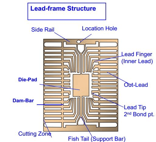
A lead frame is the central structural component of a semiconductor package. It serves three essential functions: providing a mechanical support for the silicon die, creating an electrical pathway from the die to the external circuit board, and dissipating heat generated during operation.
Copper alloys are the material of choice for high-performance applications. Pure copper offers exceptional electrical conductivity (100% IACS) but lacks the mechanical strength required for fine-pitch manufacturing and thermal cycling reliability. By adding small percentages of elements such as iron, phosphorus, nickel, or silicon, manufacturers create alloys that balance conductivity with yield strength. Common examples include:
- C194 (Cu-Fe-P): The industry workhorse, offering good strength and conductivity for general-purpose lead frames.
- C7025 (Cu-Ni-Si): A high-strength alloy with excellent stress relaxation resistance, ideal for fine-pitch and high-temperature applications.
- C151 (Cu-Zr): Provides superior thermal stability for automotive and power electronics.
These materials typically enter the manufacturing line in coil form with thicknesses ranging from 0.05 mm to 0.3 mm—a range that spans from ultra-thin consumer electronics packaging to robust automotive-grade components.
The Fine Pitch Imperative
As semiconductor packages evolve from traditional through-hole designs to surface-mount configurations, the number of input/output (I/O) connections per package continues to rise while package dimensions shrink. This trend gives rise to fine pitch—the reduction of center-to-center spacing between adjacent leads.
In practical terms, fine pitch is defined as lead spacing below 0.5 mm, with advanced applications pushing into the 0.15 mm to 0.3 mm range. The demand for fine pitch is driven by:
- Die Shrink: Smaller silicon die sizes require lead frames with proportionally finer geometries to maintain interconnection density.
- Package Miniaturization: Portable electronics demand smaller footprints without sacrificing functionality.
- High-Speed Performance: Shorter lead lengths reduce parasitic inductance and capacitance, critical for 5G, automotive radar, and high-frequency switching applications.
However, producing such dense geometries introduces significant manufacturing complexity. When lead fingers become narrower than the material thickness, traditional stamping methods encounter mechanical limitations.
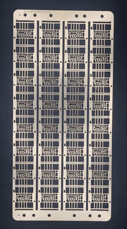
The Manufacturing Process: Step-by-Step Equipment and Function
Chemical etching, also known as photochemical machining (PCM), offers a stress-free alternative to mechanical stamping. The process is subtractive: a photoresist pattern protects the desired lead frame geometry while chemical etchant dissolves the exposed copper. Below is a detailed breakdown of each stage, including the specific equipment involved.
Step 1: Material Unwinding & Surface Preparation
Equipment: Pay-Off Reel, Alkaline Cleaning Station, Micro-Etching Unit
The process begins with a copper alloy coil mounted on a pay-off reel that maintains consistent tension. The strip passes through an alkaline cleaning station, where heated cleaning solutions remove rolling oils, oxidation, and particulate contamination. Surface cleanliness is non-negotiable—any residue compromises photoresist adhesion, leading to defects in fine-pitch features.
Following cleaning, the strip enters a micro-etching unit, typically using a sodium persulfate or sulfuric acid-based solution. This step creates a controlled surface roughness (approximately 0.5–1.0 μm Ra), significantly improving the mechanical bond between the copper and the subsequent photoresist layer.
Step 2: Photoresist Application
Equipment: Dry Film Laminator (Class 1000 Cleanroom Environment)
A dry film laminator applies a photosensitive polymer film to both sides of the strip. This occurs in a cleanroom environment to prevent airborne particles from causing pinhole defects—a critical requirement for fine pitch, where a single contaminant particle can bridge adjacent leads.
The laminator uses heated rollers (typically 100–120°C) to apply pressure and ensure complete adhesion without entrapping air bubbles. Film thickness is carefully controlled, generally between 15–38 μm, depending on the etch depth required.
Step 3: UV Exposure (Pattern Transfer)
Equipment: Double-Sided Contact Exposure Unit
The laminated strip moves into a double-sided UV exposure unit, where it is precisely aligned between two high-resolution glass phototools. These phototools contain the negative image of the lead frame pattern. High-intensity UV light (typically 365 nm or 405 nm) passes through the transparent areas of the phototool, polymerizing (hardening) the photoresist in those regions.
For fine pitch applications, exposure equipment must achieve alignment accuracy within ±5 μm to prevent “staircasing”—a condition where misalignment between top and bottom patterns results in asymmetric etch profiles.
Step 4: Developing
Equipment: Spray Developer Chamber
After exposure, the strip enters a spray developer chamber where a dilute sodium carbonate solution (0.5–1.5% concentration) is applied through oscillating spray nozzles. This solution dissolves the unexposed (non-polymerized) photoresist, revealing bare copper in the areas intended for removal.
The development process is precisely timed and temperature-controlled (typically 30–40°C) to ensure complete removal without attacking the polymerized mask. Over-development can erode fine feature edges, while under-development leaves residual resist that blocks etchant access.
Step 5: Chemical Etching
Equipment: Conveyorized Spray Etcher with Oscillating Nozzles
This is the core of the manufacturing process. The strip travels through a conveyorized spray etcher—a multi-chamber system where heated etchant (typically cupric chloride or ferric chloride) is sprayed onto both surfaces through high-pressure oscillating nozzles.
The chemistry and mechanics work together to achieve precision:
- Cupric chloride (CuCl₂): Preferred for its regeneration capability and consistent etch rates.
- Etch temperature: 45–55°C
- Nozzle pressure: 20–40 psi
For fine pitch applications, manufacturers often employ dual-sided etching with controlled undercut. Since etchant attacks laterally as well as vertically, the resulting feature width at the copper surface is wider than the resist opening. Process engineers compensate by adjusting phototool dimensions and etch parameters. Advanced control systems monitor etch depth in real-time, achieving finished tolerances of ±0.01 mm—a critical capability for fine pitch lead frames where lead width may be only 0.10 mm.
Step 6: Resist Stripping & Finishing
Equipment: Caustic Stripper Station, Cascade Rinse System, Air Knife Dryer
After etching, the now-revealed copper lead frame passes through a caustic stripper station (sodium hydroxide or proprietary stripper chemistry) that removes the hardened photoresist. The strip then moves through a cascade rinse system using deionized water to eliminate all residual chemicals—a crucial step for surface quality and subsequent plating adhesion.
Finally, air knives blow heated, filtered air across the strip to remove moisture, producing a clean, dry lead frame ready for post-processing operations such as silver or palladium plating.
Key Process Parameters
| Parameter | Specification |
|---|---|
| Material Thickness | 0.05 – 0.3 mm |
| Dimensional Tolerance | ±0.01 mm |
| Minimum Lead Width / Spacing | Down to 0.08 mm / 0.08 mm |
| Typical Alloys | C194, C7025, C151 |
| Etching Method | Dual-sided spray etching (cupric chloride) |
| Registration Accuracy | ±5 μm |
| Surface Finish After Etching | Clean, burr-free, no mechanical stress |
For a deeper understanding of process capabilities, the Photochemical Machining Institute provides comprehensive technical resources on fine-tolerance etching.
Process Comparison: Chemical Etching vs. Laser Cutting
When selecting a manufacturing method for fine-pitch lead frames, engineers typically evaluate three primary technologies: mechanical stamping, laser cutting, and chemical etching. While stamping is cost-effective for high-volume, coarse-pitch applications, it cannot achieve fine-pitch geometries without significant tool wear and mechanical burrs. The more relevant comparison lies between chemical etching and laser cutting.
| Factor | Chemical Etching | Laser Cutting (Fiber or UV) |
|---|---|---|
| Burr Formation | None—dissolution process eliminates burrs | Minimal burr possible, but heat-affected zone (HAZ) creates recast layer |
| Stress Induction | Zero mechanical stress | Thermal stress from localized heating can warp thin materials (<0.1 mm) |
| Feature Resolution | Capable of ±0.01 mm across full panel | High spot size resolution, but maintaining ±0.01 mm over large arrays requires expensive precision stages |
| Throughput | Continuous coil-to-coil processing; high volume | Serial process; slower for high-density arrays |
| Tooling Cost | Phototools: moderate cost, fast turnaround (1–2 weeks) | No physical tooling; setup cost is low but per-part cost is higher at volume |
| Material Thickness | Optimal 0.05–0.5 mm; consistent etch factor | Capable across wide thickness range, but thin materials prone to thermal distortion |
| Edge Quality | Smooth, uniform etch profile | Slight taper possible; recast layer may require post-processing |
Chemical etching holds distinct advantages for fine-pitch copper alloys. Because it is a chemical process rather than a thermal or mechanical one, it imparts no heat-affected zone and no mechanical stress—critical factors when working with thin materials (0.05–0.1 mm) where warpage would compromise downstream wire bonding. Additionally, etching’s ability to process hundreds of parts simultaneously on a continuous coil yields significant cost advantages at scale.
Laser cutting excels in prototyping and low-volume production where phototool costs cannot be justified. However, for high-volume fine-pitch lead frames requiring tolerances of ±0.01 mm across millions of units, chemical etching remains the industry standard.
Applications: Where Fine-Pitch Etched Lead Frames Deliver Value
The combination of ultra-fine geometries, stress-free processing, and tight tolerances makes chemically etched copper alloy lead frames essential across multiple high-growth industries. Below are specific applications with precise details on where these components are deployed.
Automotive Electronics
As vehicles transition to electric and autonomous architectures, the number of semiconductor devices per vehicle has increased exponentially. Etched lead frames are found in:
- Engine Control Units (ECUs): QFN (Quad Flat No-lead) packages with 0.4 mm pitch, managing fuel injection and ignition timing.
- ADAS (Advanced Driver Assistance Systems): Radar modules using high-frequency packages with lead frames etched to 0.15 mm pitch to minimize signal loss at 77 GHz.
- Battery Management Systems (BMS): Power management ICs mounted on lead frames with thicknesses of 0.20–0.25 mm to handle higher current loads.
In these applications, the lead frames are integrated into surface-mount devices placed by high-speed pick-and-place equipment onto PCBs within modules from suppliers like Bosch, Continental, and Denso.
Consumer Electronics
The smartphone and wearable markets demand the smallest possible package footprints:
- Smartphone Power Management ICs (PMICs): Micro leadframe packages (MLP) with pitch down to 0.35 mm, integrated into main boards alongside application processors.
- Wireless Charging Controllers: Thin 0.10 mm lead frames allow stacked package assembly within the limited z-height of slim devices.
- TWS (True Wireless Stereo) Earbuds: Ultra-compact QFN packages with etched lead frames enable the dense component layout required for battery, audio processor, and wireless transceiver coexistence.
These lead frames are assembled into packages by OSATs (Outsourced Semiconductor Assembly and Test) such as Amkor, ASE, and JCET, using automated die bonding and wire bonding equipment like ASM Pacific or Kulicke & Soffa wire bonders.
Medical Devices
Reliability and miniaturization intersect in medical electronics:
- Implantable Devices (Pacemakers, Neurostimulators): Etched lead frames in ceramic or molded packages with 0.20 mm pitch, requiring exceptional long-term reliability and biocompatibility.
- Surgical Navigation Systems: High-precision sensors housed in fine-pitch lead frame packages, assembled into handheld instruments.
Manufacturing for medical applications often incorporates additional plating layers (gold or palladium) applied after etching to ensure biocompatibility and corrosion resistance.
Industrial & Communications Infrastructure
- Optical Transceivers (100G/400G/800G): High-speed data communication modules utilize lead frames with extremely short lead lengths to maintain signal integrity at 56 Gbaud and above.
- Solid-State Drives (SSDs): Controller ICs in fine-pitch packages, mounted directly on the SSD PCB alongside NAND flash memory.
In data center applications, these lead frames are ultimately installed in server motherboards within networking equipment from manufacturers like Cisco, Arista, and NVIDIA.
Chemical etching machine