Chemical Etching Fine MicroEtch Screens Animation
1. What Are Chemical Etching Fine MicroEtch Screens?
In the relentless pursuit of device miniaturization and precision fluid control, engineers face a fundamental challenge: how to create ultra-fine apertures in thin metal screens without compromising material integrity. Chemical Etching Fine MicroEtch Screens—also known as photo-etched or photo chemically etched screens—represent the answer to this challenge.
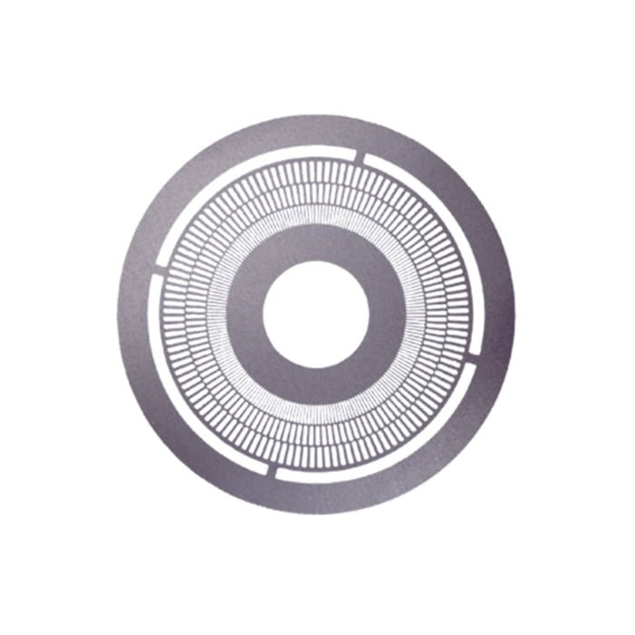
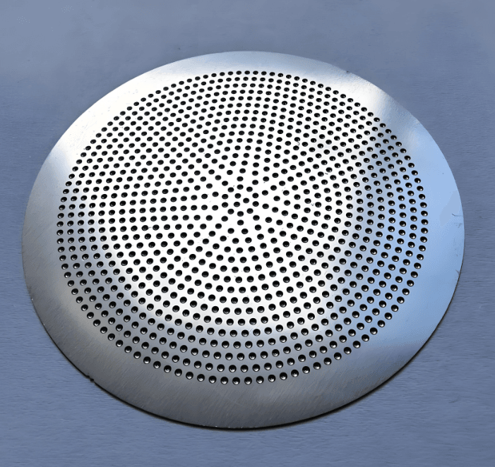
These are precision-perforated metal sheets manufactured through a controlled chemical dissolution process rather than mechanical force or thermal energy. Unlike woven wire mesh or stamped components, chemically etched screens feature burr-free apertures, no heat-affected zones (HAZ) , and unparalleled geometric consistency across large surface areas. The process begins with ultra-thin stainless steel (316L or 304) and selectively removes material where apertures are desired, leaving behind a precise micro-screen with apertures as small as 0.02 mm and tolerances reaching ±0.01 mm.
2. Why Choose Chemical Etching Over Alternative Manufacturing Methods?
The central question facing design engineers is: Why invest in chemical etching when laser cutting or stamping appear faster or cheaper?
The answer lies in the fundamental physics of each process. When precision filtration or fluid control demands zero contamination risk, perfect edge quality, and material property preservation, chemical etching proves superior.
The Problem with Laser Cutting
Laser cutting generates localized heating up to 1,200 °C at the cutting interface. This thermal input creates three critical defects:
- Heat-Affected Zones (HAZ) : The microstructure of 316L stainless steel undergoes grain growth and phase transformation around each aperture, altering mechanical properties.
- Recast Layer Formation: Molten metal resolidifies along cut edges, creating a brittle layer up to 10 μm thick that can delaminate in service.
- Micro-Burrs and Spatter: Even with optimized parameters, laser cutting produces microscopic protrusions that act as nucleation sites for particle agglomeration in filtration applications.
These flaws directly impact system performance. In semiconductor chemical mechanical planarization (CMP) slurry filtration, a single clogged aperture can cause over 4 hours of unplanned tool downtime.
The Problem with Stamping/Mechanical Punching
Mechanical processes introduce different but equally problematic defects:
- Burr Formation: Shearing action leaves burrs typically ranging 10–20 μm in height
- Work Hardening: Cold-working alters material properties around apertures
- Tool Wear: Progressive die wear causes aperture dimensions to drift over production runs
- Geometric Limitations: Minimum aperture size is constrained by punch diameter and material thickness
Why Chemical Etching Solves These Problems
Chemical etching eliminates thermal and mechanical stresses entirely. The process dissolves metal uniformly wherever the photoresist mask is absent, producing:
- Zero burrs or recast layer
- No thermal distortion or HAZ
- Preserved material microstructure (essential for biocompatibility and corrosion resistance)
- Consistent aperture geometry across the entire panel
A comparative analysis reveals the distinct advantages, as detailed in Datum Alloys’ comparison of laser cutting, chemical etching, and stamping:
| Parameter | Chemical Etching | Laser Cutting | Stamping/Punching |
|---|---|---|---|
| Minimum Aperture | 0.01 mm (10 μm) | 0.05 mm (50 μm) | 0.10 mm (100 μm) |
| Edge Condition | Burr-free, smooth | Recast layer 5–15 μm, micro-burrs | Burrs 10–20 μm, requires deburring |
| Heat-Affected Zone | None | Present (microstructure altered) | None (but work-hardened) |
| Material Stress | Zero mechanical/thermal | Thermal distortion | Mechanical stress/strain hardening |
| Tolerance Capability | ±0.01 mm typical | ±0.025–0.050 mm | ±0.025–0.075 mm (tool dependent) |
| Aperture Shape Complexity | Unlimited (any CAD-defined shape) | Limited by laser path | Constrained by punch geometry |
| Tooling Cost | Low (digital mask only) | None (programming only) | High (hard tooling required) |
| Volume Scalability | Excellent (batch processing) | Moderate (serial processing) | Excellent (high-speed stamping) |
3. The 10-Step Ultra-Fine Manufacturing Process
The precision of chemical etching micro-screens is not accidental—it results from rigorous control across ten critical stages.
Step 1: Substrate Preparation (Ultra-Clean)
Material Selection: 316L or 304 cold-rolled ultra-thin stainless steel, thickness range 0.05–0.3 mm (though capable down to 0.03 mm), with no surface scratches or oxidation.
Process Sequence: Alkaline degreasing → acid pickling (dilute HNO₃) → multi-stage deionized water rinsing → hot air drying → electrostatic dust removal.
Quality Target: Surface roughness Ra ≤ 0.1 μm, completely free of oils and oxides. This level of cleanliness ensures photoresist adhesion exceeds 48 hours under cleanroom conditions. Research by Wei et al. (2024) demonstrated that surface contamination directly correlates with pitting corrosion during etching, compromising aperture precision.
Step 2: Dual-Side Photoresist Coating (Uniformity Critical)
Resist Type: High-resolution dry film photoresist (5–10 μm thickness) or liquid negative-tone photoresist for ultra-fine linewidth applications.
Application Method: Dual-side roll coating or spin coating achieving thickness uniformity within ±0.1 μm.
Pre-bake: 80–90°C for 5–10 minutes, forming a dense, pinhole-free photosensitive layer. This step drives off residual solvents and promotes cross-linking initiation.
Step 3: High-Precision Exposure
Exposure Method: Laser Direct Imaging (LDI) or high-precision UV contact exposure with positioning error < ±1 μm. LDI offers the advantage of eliminating physical phototools, enabling rapid design iteration without film distortion concerns.
Mask: Glass chrome mask or high-precision film, CAD-defined aperture arrays with minimum linewidth/spacing ≥0.02 mm.
Process: Dual-side simultaneous exposure ensures symmetrical through-hole formation. Energy delivery is precisely controlled to achieve complete cross-linking of exposed photoresist regions without under- or over-exposure.
Step 4: Development (Precise Opening)
Developer: 1–2% sodium carbonate (Na₂CO₃) alkaline solution at 30–35°C.
Method: Spray + immersion for 30–60 seconds, completely dissolving unexposed photoresist to reveal the metal surfaces destined for etching.
Rinsing: Multi-stage deionized water rinsing removes residual developer, followed by drying.
Inspection: Optical microscopy (100–500× magnification) verifies window edge sharpness, complete resist removal, and absence of pinholes or bridging.
Step 5: Chemical Etching (Core Process)
The etching step determines final quality. This stage employs a carefully formulated etchant system specifically optimized for stainless steel.
Etchant Composition (Stainless Steel Optimized) :
- Primary: 40–45°Bé ferric chloride (FeCl₃)—strong oxidizing agent providing the primary dissolution mechanism
- Additives: 5–8% HNO₃ + 1–3% HCl—these break down the chromium oxide (Cr₂O₃) passive layer that naturally protects stainless steel, enabling controlled etching
Process Parameters:
- Temperature: 45–55°C, controlled to ±0.5°C
- Etching Method: Dual-side pulsed spray etching at 0.1–0.3 MPa pressure with 1–2 Hz frequency
- Etch Rate: 0.03–0.06 mm/min—intentionally slow to maintain precision
- Endpoint Control: Online thickness/transmittance monitoring enables precise stop point, preventing over-etching (enlarged apertures) or under-etching (incomplete penetration)
Mechanism: The isotropic nature of chemical dissolution creates smooth, taper-free sidewalls. According to Ennovi’s technical literature on enhanced chemical etching, proper formulation balances etch rate against lateral undercut to maximize the etch factor for ultra-fine apertures.
Step 6: Resist Stripping
Stripping Solution: 5–10% sodium hydroxide (NaOH) at 50–60°C, or commercial stripper formulations.
Method: Spray + ultrasonic agitation to completely remove remaining photoresist.
Cleaning: Multi-stage deionized water rinsing with ultrasonic assistance removes all chemical residues.
Step 7: Post-Treatment (Performance Enhancement)
Electropolishing (Optional) : Enhances aperture walls to Ra ≤ 0.2 μm, reducing fluid flow resistance and improving contamination resistance.
Passivation: Dilute nitric acid treatment forms a thin, dense chromium oxide layer, restoring and enhancing corrosion resistance.
Annealing (Optional) : Low-temperature stress relief annealing (<600°C in protective atmosphere) restores mechanical properties without affecting aperture dimensions.
Step 8: Precision Inspection
Dimensional Verification:
- Laser diameter measurement / optical imaging: aperture diameter ±0.01 mm, positional accuracy ±0.01 mm
- Uniformity: Coefficient of Variation (CV) ≤ 5% for aperture consistency
Visual Inspection: Microscopy at 500× confirms no burrs, pinholes, corrosion pits, or wall irregularities.
Flatness: ≤0.003 mm for thin materials—critical for proper sealing in filter housings.
Functional Testing: Bubble point or flow rate testing validates aperture consistency and permeability.
Step 9: Cutting and Profiling
Method: Laser micro-cutting or contour etching, avoiding mechanical stress that could distort ultra-thin screens.
Dimensions: Maximum panel size up to 600 × 600 mm, with custom external profiles.
Step 10: Packaging and Delivery
Method: Vacuum packaging with moisture barrier protection prevents oxidation and surface damage during transit.
4. Technical Specifications Summary
| Parameter | Capability |
|---|---|
| Material | 316L stainless steel (surgical grade), 304 stainless steel |
| Thickness Range | 0.05–0.3 mm (0.002–0.012 in) |
| Minimum Aperture | 0.02 mm (20 μm) |
| Dimensional Tolerance | ±0.01 mm (10 μm) |
| Positional Accuracy | ±0.01 mm |
| Aperture Uniformity (CV) | ≤ 5% |
| Surface Finish (post-electropolish) | Ra 0.05–0.2 μm |
| Flatness | ≤ 0.003 mm per 100 mm |
| Open Area | Up to 75% depending on pattern |
| Compliance | FDA 21 CFR 177.1520, ISO 13485, USP Class VI (when specified) |
Technical specifications based on industry-standard capabilities as outlined in TOMAI Filter’s technical overview of photo etch mesh
5. Applications: Where MicroEtch Screens Enable Critical Technology
Chemical etching micro-screens are not merely components—they are enabling technologies across industries where precision, cleanliness, and reliability are non-negotiable.
Medical Devices
| Application | Specific Use | Device/Equipment |
|---|---|---|
| IV Therapy Filtration | Sub-micron particulate removal from intravenous fluids | Infusion pumps, IV sets |
| Implantable Ports | Particle-free membranes for drug delivery | Chemotherapy ports, insulin pumps |
| Surgical Instruments | Debris shields for robotic surgery tools | Da Vinci surgical system components |
| Respiratory Therapy | Aerosol generation screens for nebulizers | Inhalers, nebulizer plates |
| Diagnostic Cartridges | Flow control membranes for lab-on-chip devices | Point-of-care diagnostic test cartridges |
In medical applications, the burr-free nature of etched screens eliminates metal shedding risk—a critical safety factor for implantable devices subject to >10,000 autoclave cycles.
Semiconductor Manufacturing
| Application | Specific Use | Device/Equipment |
|---|---|---|
| CMP Slurry Filtration | 0.2 μm particle removal protecting polishing pads | Chemical mechanical planarization tools |
| Gas Diffusion | Uniform pore distribution for wafer processing | Gas diffusers in 100–300 mm wafer tools |
| Photoresist Filtration | Contaminant removal in lithography | Coater/developer track systems |
| Wet Etch Processing | Basket and carrier screens | Wet bench processing equipment |
Semiconductor applications demand CV ≤ 5% aperture uniformity to ensure consistent flow distribution across wafer surfaces—a specification unachievable with woven mesh.
Aerospace and Defense
| Application | Specific Use | Device/Equipment |
|---|---|---|
| Hydraulic Filtration | Contamination control meeting SAE AS4059F | Aircraft hydraulic systems |
| Fuel System Screens | Debris prevention in fuel lines | Fuel pumps, injectors |
| EMI/RFI Shielding | Precision shielding for avionics | Communication systems, radar |
| Cooling Systems | Flow control in thermal management | Liquid cooling loops |
Aerospace applications rely on the material integrity preserved by etching—no HAZ means no weak points in high-vibration environments.
Analytical Instruments
| Application | Specific Use | Device/Equipment |
|---|---|---|
| HPLC Filtration | In-line solvent filtration | High-performance liquid chromatography systems |
| Mass Spectrometry | Sample introduction screens | LC-MS, GC-MS instruments |
| Particle Analysis | Sieving screens for calibration | Laser diffraction particle analyzers |
| Gas Chromatography | Flow control membranes | GC injector systems |
Appliance and Water Management
| Application | Specific Use | Device/Equipment |
|---|---|---|
| Water-Efficient Appliances | Flow restriction screens | Dishwashers, washing machines |
| Water Filtration Systems | Sediment and particulate removal | Reverse osmosis systems, water dispensers |
| Coffee Machines | Aeration and distribution screens | Commercial espresso equipment |
The appliance industry increasingly adopts etched screens to enable water-saving designs that reduce consumption by up to 30% while maintaining user experience.
Emerging Applications
| Application | Specific Use | Device/Equipment |
|---|---|---|
| Fuel Cells | Hydrogen distribution plates | PEM fuel cell stacks |
| 3D Printing | Metal powder sieving for additive manufacturing | Powder bed fusion systems |
| 5G Telecommunications | Waveguide and RF shielding components | 5G base station antennas |
| Microfluidics | Lab-on-chip flow control | Point-of-care diagnostic devices |
6. Conclusion
Chemical Etching Fine MicroEtch Screens represent the convergence of material science, precision photolithography, and controlled chemical processing to solve engineering challenges that thermal and mechanical methods cannot address. For applications demanding ultra-fine apertures (down to 0.02 mm) , zero burr edges, preserved material properties, and uncompromising cleanliness, chemical etching is not merely an alternative—it is the enabling technology.
When your filtration, fluid control, or precision component application requires tolerances of ±0.01 mm in materials as thin as 0.05 mm, the question is not whether to consider chemical etching, but whether you can afford to specify anything else.
Chemical etching machine