Advanced nanoporous SiO2 coatings for ultraviolet laser-resistant optics
As high-power ultraviolet (UV) laser systems push into new industrial and scientific frontiers, the durability of optical components under intense irradiation has become a critical bottleneck. Advanced nanoporous silicon dioxide (SiO2) coatings are emerging as a promising solution to enhance the laser damage resistance of optics, according to recent developments highlighted in EIN News.
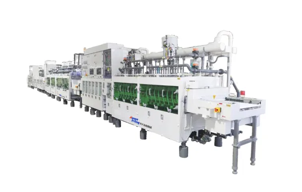
The coatings leverage precisely engineered nanoscale pores to reduce electron excitation and thermal buildup, mitigating the primary failure modes that plague conventional dense films when exposed to short-wavelength, high-energy laser pulses. Researchers are increasingly turning to chemical etching machine processes to create these structured layers with controlled porosity and thickness.
The Challenge of UV Laser-Induced Damage

Ultraviolet lasers operating at wavelengths below 355 nm are essential for semiconductor lithography, precision machining, and medical procedures. However, the photon energy at these wavelengths is sufficient to cause nonlinear absorption, defect generation, and ultimately catastrophic breakdown of the optical coatings that steer and focus the beam. Traditional dense oxide films tend to crack or delaminate under repeated thermal cycling, limiting component lifetime and driving up maintenance costs.
Engineers have long sought materials with both low absorption coefficients and high mechanical resilience. Nanoporous SiO2 addresses these requirements by introducing a sacrificial microstructure that can absorb stress while maintaining optical clarity. The approach builds on decades of thin-film research but has gained new traction thanks to advanced etching and templating techniques.
How Nanoporous SiO2 Coatings Work
Creating functional nanoporous silica layers involves a multi-step process that often includes sol-gel deposition followed by selective chemical etching. The resulting film features an interconnected network of voids that can be tailored in size from a few nanometers to tens of nanometers. This architecture confers several key advantages:
- Reduced effective refractive index, enabling better antireflective performance and broader angular acceptance.
- Higher laser-induced damage thresholds due to efficient heat dissipation through the pore network.
- Enhanced mechanical compliance, allowing the coating to expand and contract without cracking.
- Compatibility with various substrate materials including fused silica, crystalline quartz, and certain glasses.
Wet chemical etching machines are frequently employed to selectively remove a sacrificial phase from a two-phase composite, leaving behind the porous silica framework. By adjusting etchant concentration, temperature, and processing time, manufacturers can precisely control the final pore structure and film homogeneity. Subsequent heat treatments may be applied to stabilize the coating and remove any residual organic templates.
Industry Implications and Future Outlook
The commercial availability of UV lasers with higher average powers and longer service intervals would accelerate adoption in fields such as advanced packaging, flat-panel display production, and reflective surgery. Optical component suppliers are actively evaluating nanoporous coatings to qualify them for next-generation lithography systems that operate at 193 nm and beyond.
While the concept is not entirely new, recent process improvements have made nanoporous SiO2 films more reproducible and scalable. Several research groups and manufacturers are reported to be scaling up deposition systems to coat large-area optics, aiming for defect densities low enough for high-yield manufacturing.
The development of durable UV laser optics through nanoporous SiO2 coatings represents a meaningful advance in optical material science, with the potential to extend the operational lifespan of critical laser components and enable new applications that demand higher reliability under extreme conditions.
Why This Matters
This innovation directly addresses the lifetime and reliability challenges of UV optics in semiconductor fabrication and medical lasers, potentially reducing downtime and enabling higher-energy laser systems. It could reshape optical component design for next-generation excimer and solid-state UV sources.
FAQ
Why are nanoporous SiO2 coatings needed for UV laser optics?
Conventional dense coatings degrade under high-energy UV pulses due to thermal and electronic stress. Nanoporous structures mitigate these effects by providing stress relief and improved heat dissipation, leading to longer component life and higher damage thresholds.
How is chemical etching used in creating nanoporous SiO2 films?
Chemical etching selectively removes a sacrificial component from a deposited composite film, leaving behind a porous silica network. Wet chemical etching machines provide precise control over pore size and film uniformity through adjustments to etchant chemistry and process parameters.
What are the main benefits of nanoporous over traditional optical coatings?
Nanoporous coatings offer lower refractive indices, higher laser damage thresholds, and greater mechanical flexibility. They can be tailored for specific wavelengths and substrates, improving overall optical system performance while reducing failure rates under pulsed UV irradiation.
Which industries will benefit most from these advanced coatings?
Semiconductor lithography, medical laser surgery, and materials processing industries stand to gain significantly, as they rely on high-power UV lasers where optics lifetime is a critical cost factor. Enhanced durability also benefits scientific research and defense applications.
Source: "chemical etching" – Google News