Etching Chemicals Market Projected to Hit $52 Billion by 2033 Amid Semiconductor Boom
By the Numbers
This story carries monetary or market figures such as $52 Billion and US$52.0 billion. They are the kind of detail worth noting up front, then confirming against the original report for exact amounts and scope.
- Market value: $52 Billion Etching Chemicals Market Projected to Hit $52 Billion by 2033 Amid Semiconductor Boom A new market analysis projects the global etching chemicals industry will reach US$52.0 billion by 2033, with semiconductor manufacturing…
- Market value: US$52.0 billion These trends, coupled with unrelenting semiconductor demand, are expected to sustain a compound annual growth rate that lifts the market to US$52.0 billion by 2033.
The global etching chemicals landscape underpins the precision manufacturing of integrated circuits and microelectromechanical systems. From wet solutions to dry plasma chemistries, these materials enable the selective removal of layers on silicon wafers with nanometre accuracy. A newly released industry analysis now puts a firm figure on this growth trajectory.
Semiconductor Expansion Fuels Etching Chemical Demand

Escalating production of logic, memory, and analog chips is driving consumption of high-purity etchants. Fabrication plants are ramping up capacity to meet orders from automotive electronics, data centres, and 5G infrastructure. Each advanced node requires more etching steps, increasing the volume of chemistries consumed per wafer.
Specialised mixtures for silicon, oxide, and metal layers are being reformulated to handle complex 3D architectures such as FinFETs and gate-all-around transistors. The shift towards vertical integration and multi-patterning further amplifies chemical throughput. Suppliers are expanding their portfolios to address specific material stacks and contamination control requirements.
Asia-Pacific Dominates Production and Consumption
Taiwan, South Korea, and mainland China collectively account for the largest share of global etching chemical usage. Massive foundry clusters and memory gigafabs in these nations consume tens of thousands of tonnes annually. Government subsidies and technology transfer agreements continue to attract new investments in local chemical purification facilities.
Japan and Singapore are also strengthening their roles as high-purity chemical exporters. Regional logistics networks enable just-in-time delivery to semiconductor lines, reducing inventory risks. Meanwhile, the United States and Europe are incentivising domestic supply chains to mitigate geopolitical concentration.
Advanced Node Technologies Boost High-Purity Chemical Requirements
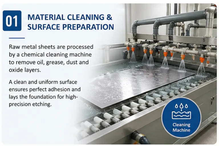
Node transitions below 5 nanometres demand etchants with contaminant levels measured in parts per trillion. Even trace metals can degrade transistor performance, pushing chemical manufacturers to refine distillation and packaging processes. Chemical etching machines play a pivotal role in processing these ultra-clean formulations, ensuring consistent quality at high throughput.
Atomic-layer etching chemistries are gaining traction for their ability to remove material one atomic layer at a time. Such precision is indispensable for defining features in next-generation devices. Research consortia are collaborating with chemical producers to design gases and solvents that minimise environmental footprint while maximising selectivity.
Sustainability and Supply Chain Resilience Gain Focus
Regulatory pressure is steering the market towards low-global-warming-potential etch gases and closed-loop recycling systems. Fabs are adopting abatement technologies that capture perfluorinated compounds before release. Chemical firms are investing in green chemistry principles to develop biodegradable or easily scrubbed alternatives.
Dual-sourcing strategies and multi-region manufacturing are becoming the norm to buffer against disruptions like natural disasters or trade disputes. Digital platforms that track chemical provenance and carbon intensity are emerging as tools for compliance and operational efficiency. These trends, coupled with unrelenting semiconductor demand, are expected to sustain a compound annual growth rate that lifts the market to US$52.0 billion by 2033.
The forecast underscores the deep interconnection between chip fabrication and specialty chemical innovation, with etching materials remaining a cornerstone of technological progress.
Why This Matters
This forecast highlights the etching chemicals market as a direct beneficiary of semiconductor megatrends. As chips power everything from AI accelerators to electric vehicles, the demand for ultra-pure chemical formulations intensifies, making material science a critical enabler of Moore’s Law progress and digital sovereignty.
FAQ
What factors are driving the etching chemicals market growth?
The primary driver is expanding semiconductor fabrication, especially for advanced logic and memory chips. Additional factors include increasing etch steps per wafer, the rise of 3D transistor architectures, and the need for high-purity chemicals to reduce defects. Regional capacity build-outs and government incentives also contribute.
Which regions lead in etching chemicals consumption?
Asia-Pacific dominates, with Taiwan, South Korea, China, and Japan collectively responsible for the majority of consumption. These countries host the world’s largest foundry and memory manufacturing bases, supported by well-established chemical supply chains and logistics networks.
How does semiconductor miniaturization affect etching chemical demand?
Smaller nodes require more etching steps and tighter contamination control, increasing the volume and value of chemicals used. Technologies like atomic-layer etching demand highly specialised chemistries that can remove material with atomic precision without damaging neighboring structures.
What are the main types of etching chemicals used in semiconductor manufacturing?
Common types include wet chemicals such as hydrofluoric acid, nitric acid, and phosphoric acid for silicon and oxide etching, as well as dry etch gases like fluorocarbons, chlorine, and bromine compounds. Advanced nodes also use proprietary mixtures and atomic-layer etching precursors tailored to specific materials.