Chemical Etching Tungsten Electron Grids Animation
Tungsten is prized for its high melting point (3,422 °C) and low vapor pressure, making it an ideal candidate for electron-emitting components. Yet, its inherent brittleness makes traditional cutting nearly impossible. This is why chemical etching, or Photochemical Machining (PCM), has become the industry standard for creating the high-precision grids that power our most advanced vacuum and beam technologies.
What are Chemical Etched Robust Electron Grids?
An electron grid is a fine, mesh-like structure used to control the flow of electrons within a vacuum environment. When we speak of “robust” Tungsten grids, we are referring to components that maintain their structural geometry despite intense thermal cycling.
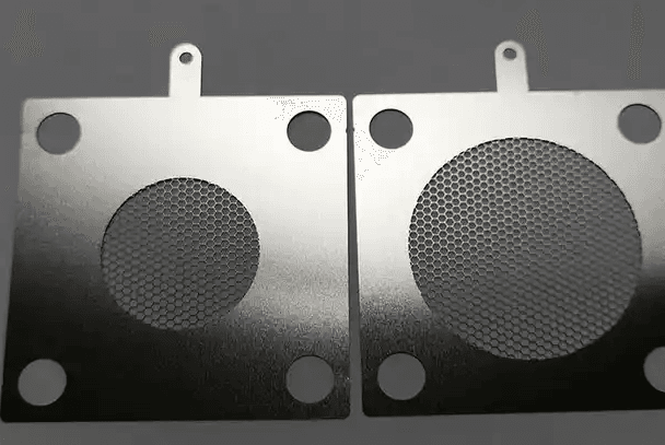
Unlike mechanical weaving, which can create uneven tension, photochemical machining produces these grids from a single, solid sheet of Tungsten. A digital mask is applied, and a specialized chemical etchant (often a strong alkaline solution) dissolves the unwanted metal. The result is a monolithic grid with perfectly uniform openings, ensuring a consistent electron field without the “hot spots” caused by mechanical inconsistencies.
Why is Chemical Etching Necessary for Tungsten?
Tungsten doesn’t just “resist” machining; it fights back. If you try to punch or mill it, the material often shatters like glass.
- Elimination of Micro-Cracks: Tungsten is highly sensitive to mechanical stress. Conventional stamping creates micro-fractures at the edges. Under the high heat of an electron gun, these cracks expand, leading to catastrophic grid failure. Etching is a “stress-free” process that keeps the crystal structure intact.
- Thermal Stability: Because etching is a “cold” process, it doesn’t create a Heat-Affected Zone (HAZ). This ensures that the Tungsten’s naturally high recrystallization temperature remains uniform across the entire grid, preventing the part from sagging or warping during operation.
- Complex Transparency: For high-efficiency electron guns, you need a high “transparency” (more hole than metal). Etching allows for incredibly thin “web” widths between holes that would be too fragile for a laser or a drill.
Process Comparison: Chemical Etching vs. Electrical Discharge Machining (EDM)
While EDM is often used for hard metals, it struggles with the high-volume and thin-gauge requirements of electron grids.
| Feature | Chemical Etching | Wire EDM |
| Throughput | High (Sheets etched at once) | Low (Part-by-part) |
| Material Stress | Zero | Thermal (Recast layer) |
| Feature Detail | Extremely Fine | Limited by wire diameter |
| Surface Finish | Smooth & Clean | Rough (requires polishing) |
| Design Flexibility | Complex patterns are “free” | High cost for complexity |
Technical Data and Precision Standards
To control a beam of electrons, the grid must be a masterpiece of geometry. Chemical etching delivers the sub-millimeter accuracy required for high-vacuum electronics:
- Thickness Range: $0.05-0.3mm (Balancing electron transparency with structural rigidity).
- Dimensional Tolerance: +- 0.01mm (Ensuring perfect alignment of the electron beam).
- Edge Geometry: Taper-controlled edges for optimized field emission.
Critical Applications: From Medical Imaging to Deep Space
Chemical etched Tungsten grids are the “gatekeepers” of energy in several high-stakes pieces of equipment:
1. Medical X-Ray and CT Scanners
In high-output X-Ray Tubes, Tungsten grids are used to focus and gate the electron beam as it strikes the anode. The +- 0.01mm tolerance ensures that the resulting image is sharp, allowing doctors to detect fractures or tumors with absolute clarity.
2. Satellite Ion Propulsion
In Hall Effect Thrusters and Ion Engines, Tungsten grids are used to accelerate ions for deep-space travel. These grids must survive years of constant thermal bombardment. Because etched Tungsten doesn’t warp, the thruster maintains a consistent trajectory for the satellite over its entire decade-long mission.
3. Semiconductor Manufacturing
Tungsten grids are utilized in Ion Implantation Equipment. These machines “shoot” ions into silicon wafers to create microchips. The precision of the etched grid ensures that the ions are distributed with perfect uniformity, preventing defects in the chips that power our smartphones and AI servers.
By bypassing the mechanical “brute force” of traditional tools, chemical etching unlocks the true potential of Tungsten—providing the thermal stability and precision required for the future of vacuum science.
Chemical etching machine